How Single Pulse Mode in Boost Converter Saves the Output Capacitor
Trademarks
All trademarks are the property of their respective owners.
1 Traditional Power-Save Mode Control Scheme
The traditional power-save mode use a low power voltage comparator to enable and disable the control loop under light load. When the output voltage reaches the target value, all the internal blocks will be disabled except the voltage comparator and reference voltage. It is fundamentally a burst-mode-control topology. In systems whose output load is at the boundary of power save mode and normal PWM mode, the device can turn on and off the control loop a number of times. To minimize the probability of the device switch between these two modes, a high hysteresis is added. Then DC output voltage is higher than the nominal value in such kind of control schemes. Typically, the DC voltage in power save mode is 0.5% to 3% higher than the nominal value. Take the TPS61021A as the example, Figure 1-1 is the typical operation behaviors of TPS61021A at light load.
 Figure 1-1 Traditional Power Save Mode
Control Scheme
Figure 1-1 Traditional Power Save Mode
Control SchemeWhen the output load decreases, the error amplifier output is clamped at a certain level. Then the output voltage increases and the devices enters power save mode. During the switching period, the control loop is active and continue to output switching signals until the output voltage hits the PFM reference voltage (0.8% percent higher than the nominal voltage). Then the control loop commands the device stopping switching but actually the device will continue to switch for some cycles because of the internal comparator delay. After that, the device stops switching finally. During the non-switching period, the load is supplied by the output capacitor and the output voltage declines. When the FB voltage drops below the PFM reference voltage, the device starts switching again to ramp up the output voltage after some delay time of the comparator,.
This control scheme is very simple and effective, but it introduces high output ripple because of the multiple switching pulses in one power save mode cycle.
2 Single Pulse Power Save Mode Control Scheme
The TPS61322xx is a low quiescent, high efficiency synchronous boost converter family based on hysteretic current control topology. The TPS61322xx is designed for systems which need a constant on and quiet power rail. The input source can be one cell alkaline battery, CR2032, and lithium battery. Figure 2-1 shows the typical application schematic of TPS61322xx.
 Figure 2-1 Single Pulse Control Scheme
The TPS61322xx uses single pulse power save mode and keeps the output voltage the same over all the load range. The typical control scheme is shown in Figure 2-2
 Figure 2-2 Single Pulse Control Scheme
There are 3 operation subintervals for TPS61322xx at light load: on-phase, off-phase and stop-phase. During on-phase, the low-side MOSFET is ON and high-side MOFET is OFF, the input source charges the inductor and the subsystem is powered by the output capacitor. The inductor current ramps up until triggers the hysteresis current Ihys, then the on-phase ends and the off-phases starts. During off-phase, the low-side MOSFET is OFF and high-side MOSFET is ON. The inductor charges the output capacitor and powers the sub-system at the same time. The inductor current ramps down until trigger zero current, then the stop-phase starts. During stop-phase, both low-side and high-side MOSFET are OFF and all the energy is from the output capacitor. The internal control loop is always active and regulate the stop-phase time.
This control scheme helps reduce the output capacitor significantly because only one current pulse is output in each power save mode cycle.
3 Output Ripple Calculation
The TPS613221A, a 3.3-V version from TPS61322xx family is used as the example.
To simplify the calculation, there is no load at the output of TPS613221A, and the efficiency is 100%. All the input energy on the inductor will be discharged to the output capacitor. From the power balance point, the energy discharged to the output capacitor is shown in Equation 1:

where

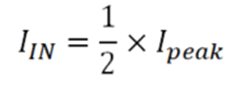
The peak inductor current at light load is calculated according to the Equation 2:

where
- L is the power inductor inductance
- Ihys is 80 mA typically
- tdelay is 120 ns typically
The inductor current pulse period is calculated according to Equation 2:

where


Finally, the output ripple will be a little higher because of the ESR in the output capacitor, which can be calculated as follow:

where
- ESR is the equivalent series resistance of the output capacitor.
When the input voltage is 1.8 V, the peak inductor current will be 200 mA according to the previous equations. The output ripple is 7.6 mV (ΔV = 6 mV, ESR × Ipeak is 1.6 mV) when using a 10-µF output capacitor with 8-mΩ ESR.