SLVAE87A December 2020 – October 2023 BQ79600-Q1 , BQ79612-Q1 , BQ79614-Q1 , BQ79616-Q1 , BQ79652-Q1 , BQ79654-Q1 , BQ79656-Q1
- 1
- Abstract
- Trademarks
- 1 NPN LDO Supply
- 2 AVDD, CVDD outputs and DVDD, NEG5, REFHP and REFHM
- 3 OTP Programming
- 4 Cell Voltage Sense (VCn) and Cell Balancing (CBn)
- 5 Bus Bar Support
- 6 TSREF
- 7 General Purpose Input-Output (GPIO) Configurations
- 8 Base and Bridge Device Configuration
- 9 Daisy-Chain Stack Configuration
- 10Multi-Drop Configuration
- 11Main ADC Digital LPF
- 12AUX Anti Aliasing Filter (AAF)
- 13Layout Guidelines
- 14BCI Performance
- 15Common and Differential Mode Noise
- 16Revision History
9.2 Ring Communication
The daisy chain communication for the device allows for the use of a ring architecture. In this architecture, a cable break between two devices does not prevent communication to all upstream devices as in a normal non-ring scheme. When the host detects a broken communication interface, the device allows the host to switch the communication direction to communicate with devices on both sides of the break. This allows for safe operation until the break in the lines is repaired.
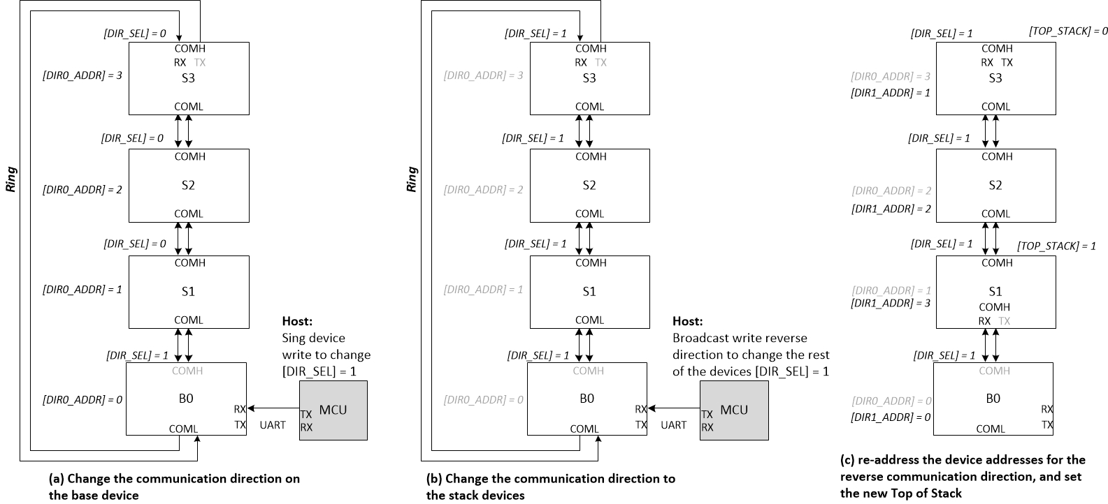
The CONTROL1[DIR_SEL] controls the communication direction. The devices will reconfigure the COMH and COML ports depends on the [DIR_SEL] and the [TOP_STACK] setting. The auto addressing procedure is needed to re-address the device addresses for the reverse communication direction.
Following is an example on how to change the communication direction to [DIR_SEL] = 1 to the entire daisy chain.
- Host clears the previous Top of
Stack device
- In this step, the previous TOS device will re-enable its COMH.
- Host sends single device write to
change the base device [DIR_SEL] = 1 (see figure (a) in Figure 9-7)
- The base device will disable its COMH and enable its COML
- Host sends broadcast write reverse
direction to change the rest of the devices’ [DIR_SEL] = 1 (see figure
(b) in Figure 9-7)
- In this step, the entire daisy chain is set up to communicate in the [DIR_SEL] = 1 direction (i.e. each device set up to transmit command frames sent by host from its COMH to its COML)
- Host performs auto addressing
procedure to set up device address in the DIR1_ADDR register (see figure (c) in
Figure 9-7)
- Unless the devices have been reset, host can skip the dummy read/write steps to synchronize the DLL in the auto addressing procedure
- Host sets up the new Top of
Stack device (see figure (c) in Figure 9-7)
- In this step, the new ToS device disables the COML transmitter
 Figure 9-7 Example of Changing
Communication Direction in Daisy Chain
Figure 9-7 Example of Changing
Communication Direction in Daisy ChainRing architecture also enables fault status transmitting in sleep. In SLEEP mode, the following fault detections are still active.
- Customer and Factory OTP shadowed registers CRC check
- Device thermal warning
- Power supplies OV, UV, oscillation detection
- If OVUV protectors are enabled, cell OV and UV detection
- If OTUT protectors are enabled, thermistors OT and UT detection
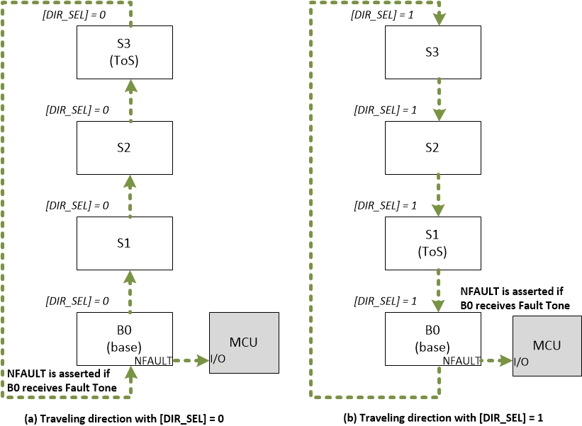
Since communication is not available in SLEEP, the device provides an option to transmit the fault status through Heartbeat (device in no fault state) and Fault Tone (device in fault state). These tones are transmitted in the same direction as a communication command frame, which is based on the CONTROL1[DIR_SEL] setting. In order for the tone signal to return back to the base device (so NFAULT can be triggered if needed), a ring architecture must be used in order to support transmitting the fault status in SLEEP mode.
 Figure 9-8 Heartbeat or Fault Tone
Traveling Direction