SLVAED3A July 2019 – April 2024 TPS568230
3 Output Ripple
The buck converter has an inherent switching action, which causes the currents and voltages in the circuit to fluctuate. The output voltage also has ripple on top of the regulated steady-state DC value. Designers of power systems consider the output voltage ripple to be a key parameter for design considerations. This section presents a brief formula for the output voltage ripple and an analysis the relationship with switching frequency.
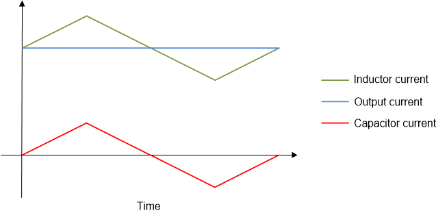
The switching action of the synchronized MOSFET causes the current in the inductor to have a triangular waveform. The DC component of the inductor current flows through the output load, and the AC portion of the inductor flow through the output capacitor, as shown in Figure 3-1. The time-varying current through the capacitor causes the voltage across the capacitor to be perturbed[3].
 Figure 3-1 Current in the Buck
Converter
Figure 3-1 Current in the Buck
ConverterThe D-CAP3 mode control technology allows the use of ceramic output capacitors with low ESR. The Output Ripple Voltage for Buck Switching Regulator Application Report (SLVA630) presents an accurate, yet easy-to-implement, formula for the output voltage ripple under low ESR condition. At light load condition, the converter operates in power skip mode (PSM) and the output voltage ripple is dependent on the output capacitor and inductor value. A larger output capacitor and inductor values minimize the voltage ripple in PSM mode. At heavy load conditions, the device operates in PWM mode. Since ceramic capacitors have extremely low ESR and relatively little capacitance, the overall output voltage ripple is the sum of the voltage spike caused by the output capacitor ESR plus the voltage ripple caused by charging and discharging the output capacitor:
Noting that:
where
- Iripple is the inductor current ripple
- C is the capacitance of the output capacitor
- R is the equivalent series resistance (ESR) of the output capacitor
- D is the duty cycle of switching
- Vout is the output voltage
For quick calculation, a simpler model of output voltage ripple is assumed. The total output ripple is the linear sum of the voltage ripple due to the capacitor alone and the voltage ripple due to resistor alone:
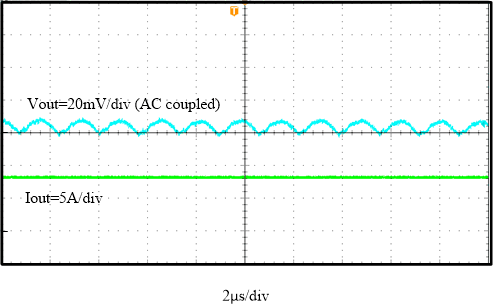
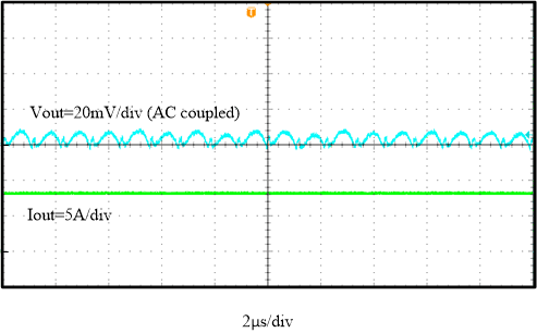
Equation 6 and Equation 7 reveal that the total output ripple is mainly affected by duty cycle, output capacitor, and inductor. Another important factor is switching frequency. Higher frequency is of great benefit for reducing output voltage ripple. Based on the parameters in Table 2-1, Figure 3-2, and Figure 3-3 show the ripple test results with 8 A loading. The ripple is 11 mV under 600 kHz and 10 mV under 1000 kHz. The ripple becomes smaller even though using the output power stage (LC) with smaller inductance and capacitance increases the switching frequency.
 Figure 3-2 Output Voltage Ripple,
FSW = 600 kHz
 Figure 3-3 Output Voltage Ripple,
FSW = 1000 kHz