SLVAFI8 February 2023 TLC6C5748-Q1
- Abstract
- Trademarks
- 1Introduction
-
2Design Considerations for Low EMI
- 2.1 Design Considerations Overview
- 2.2
Considerations in Detail
- 2.2.1 Top-Level Architecture
- 2.2.2
High Frequency Signals
- 2.2.2.1 Original Setup
- 2.2.2.2 3.3 V I/O Voltage Instead of 5 V
- 2.2.2.3 Use Independent OSC for GSCLK With Spread Spectrum
- 2.2.2.4 Without Using Buffer on GSCLK
- 2.2.2.5 Using Snubber on GSCLK
- 2.2.2.6 Lower the Signal Frequency
- 2.2.2.7 Placement and PCB layout
- 2.2.2.8 ESD Enhancement
- 2.2.2.9 Demo and Test Results
- 2.2.2.10 Bench Test Results
- 3Summary
- 4References
2.2.2.2 3.3 V I/O Voltage Instead of 5 V
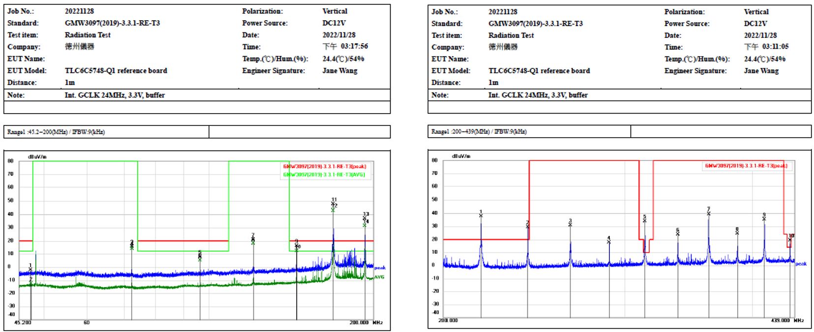
Although TLC6C5748-Q1 is compatible with either 3.3 V or 5 V I/O voltage on the interface (LAT, SIN, SCLK, GSCLK), 3.3V I/O voltage leads to lower energy in full frequency range. #FIG_TW3_BKL_FWB shows the 3.3 V I/O test results.
 Figure 2-4 Test Results of Using 3.3 V IO
Voltage Setup(Vertical Direction) from 45 MHz to 439 MHz