SLVAFI8 February 2023 TLC6C5748-Q1
- Abstract
- Trademarks
- 1Introduction
-
2Design Considerations for Low EMI
- 2.1 Design Considerations Overview
- 2.2
Considerations in Detail
- 2.2.1 Top-Level Architecture
- 2.2.2
High Frequency Signals
- 2.2.2.1 Original Setup
- 2.2.2.2 3.3 V I/O Voltage Instead of 5 V
- 2.2.2.3 Use Independent OSC for GSCLK With Spread Spectrum
- 2.2.2.4 Without Using Buffer on GSCLK
- 2.2.2.5 Using Snubber on GSCLK
- 2.2.2.6 Lower the Signal Frequency
- 2.2.2.7 Placement and PCB layout
- 2.2.2.8 ESD Enhancement
- 2.2.2.9 Demo and Test Results
- 2.2.2.10 Bench Test Results
- 3Summary
- 4References
2.2.2 High Frequency Signals
As discussed in previous sections, the pulse signals on the interface could be a noise source of EMI. Theoretically, a PWM signal with limited slew rate (shown as #FIG_CSL_H3L_FWB) could be written into Fourier series format as,
 Figure 2-1 PWM Signal Diagram
Equation 2.
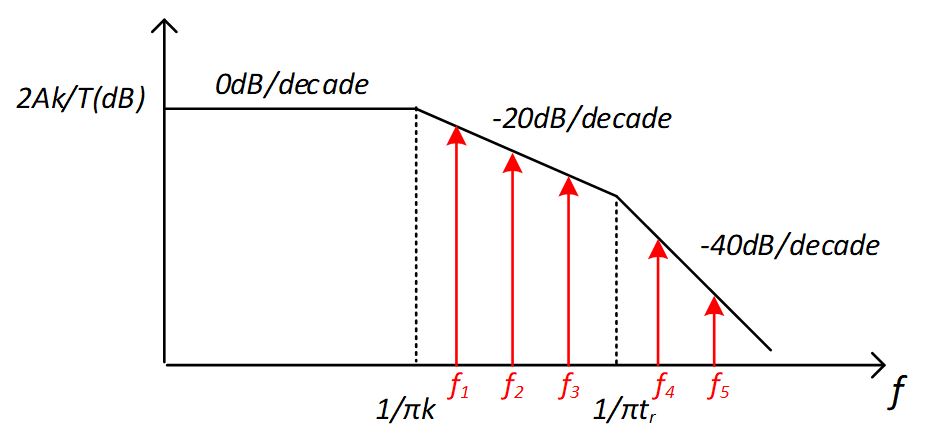
To mitigate the EMI problem from noise source, E.Q 2 indicates several approaches to lower the energy in high frequency range. #FIG_CRH_43L_FWB shows the spectrum in frequency domain.
 Figure 2-2 Fourier Series in Frequency
Domain