SLVSER3A November   2018  – April 2020 TPS65982BB

PRODUCTION DATA.  

  1. Features
  2. Applications
  3. Description
    1.     Device Images
      1.      Simplified Diagram
  4. Revision History
  5. Pin Configuration and Functions
    1.     Pin Functions
  6. Specifications
    1. 6.1  Absolute Maximum Ratings
    2. 6.2  ESD Ratings
    3. 6.3  Recommended Operating Conditions
    4. 6.4  Thermal Information
    5. 6.5  Power Supply Characteristics
    6. 6.6  Power Supervisor Characteristics
    7. 6.7  Power Consumption Characteristics
    8. 6.8  Port-Power Switch Characteristics
    9. 6.9  Port-Data Multiplexer Characteristics
    10. 6.10 Port-Data Multiplexer Clamp Characteristics
    11. 6.11 Port-Data Multiplexer Signal Monitoring Pullup and Pulldown Characteristics
    12. 6.12 USB Endpoint Characteristics
    13. 6.13 Input/Output (I/O) Characteristics
    14. 6.14 I2C Slave Characteristics
    15. 6.15 Thermal Shutdown Characteristics
    16. 6.16 Oscillator Characteristics
    17. 6.17 SPI Master Switching Characteristics
    18. 6.18 Typical Characteristics
  7. Parameter Measurement Information
  8. Detailed Description
    1. 8.1 Overview
    2. 8.2 Functional Block Diagram
    3. 8.3 Feature Description
      1. 8.3.1  Port-Power Switches
        1. 8.3.1.1 5-V Power Delivery
        2. 8.3.1.2 5-V Power Switch
        3. 8.3.1.3 PP_5V0 Current Limit
        4. 8.3.1.4 VBUS Transition to VSAFE0V
      2. 8.3.2  USB Port-Data Multiplexer
        1. 8.3.2.1 Port Multiplexer Clamp
        2. 8.3.2.2 USB2.0 Low-Speed Endpoint
      3. 8.3.3  Power Management
        1. 8.3.3.1 Power-On and Supervisory Functions
      4. 8.3.4  Digital Core
      5. 8.3.5  Power Reset-Control Module (PRCM)
      6. 8.3.6  Interrupt Monitor
      7. 8.3.7  I2C Slave
      8. 8.3.8  SPI Master
      9. 8.3.9  Thermal Shutdown
      10. 8.3.10 Oscillators
    4. 8.4 Device Functional Modes
      1. 8.4.1 SPI Master Interface
      2. 8.4.2 I2C Slave Interface
        1. 8.4.2.1 I2C Interface Description
        2. 8.4.2.2 I2C Clock Stretching
        3. 8.4.2.3 I2C Address Setting
        4. 8.4.2.4 Unique-Address Interface
        5. 8.4.2.5 I2C Pin Address Setting
  9. Application and Implementation
    1. 9.1 Application Information
    2. 9.2 Typical Application
      1. 9.2.1 VBUS Load Switch
      2. 9.2.2 HRESET
      3. 9.2.3 Dual Port Billboard Support
  10. 10Power Supply Recommendations
    1. 10.1 3.3-V Power
      1. 10.1.1 1VIN_3V3 Input Switch
      2. 10.1.2 VOUT_3V3 Output Switch
    2. 10.2 1.8-V Core Power
      1. 10.2.1 1.8-V Digital LDO
      2. 10.2.2 1.8-V Analog LDO
    3. 10.3 VDDIO
      1. 10.3.1 Recommended Supply Load Capacitance
  11. 11Layout
    1. 11.1 Layout Guidelines
    2. 11.2 Layout Example
      1. 11.2.1 Component Placement
      2. 11.2.2 Recommended Via Size and Trace Widths
      3. 11.2.3 USB2 Routing
      4. 11.2.4 Oval Pad for BGA Fanout
      5. 11.2.5 Top and Bottom Layer Complete Routing
  12. 12Device and Documentation Support
    1. 12.1 Documentation Support
      1. 12.1.1 Related Documentation
    2. 12.2 Receiving Notification of Documentation Updates
    3. 12.3 Support Resources
    4. 12.4 Trademarks
    5. 12.5 Electrostatic Discharge Caution
    6. 12.6 Glossary
  13. 13Mechanical, Packaging, and Orderable Information

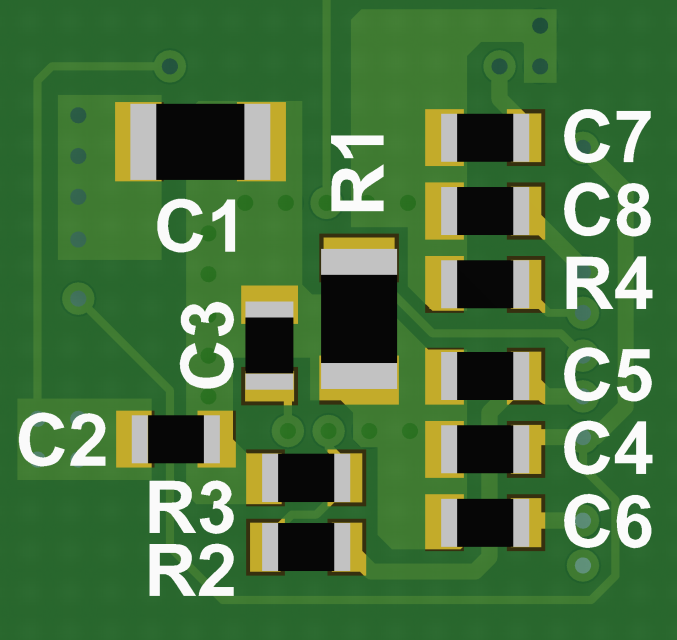
Component Placement

The recommended placement is to have the TPS65982BB on the Top Layer and have all of the passive components on the opposite layer of the PCB. This will significantly reduce solution size and allows for more clearance for the high speed and interface signals. The figures below show the top and bottom placement.
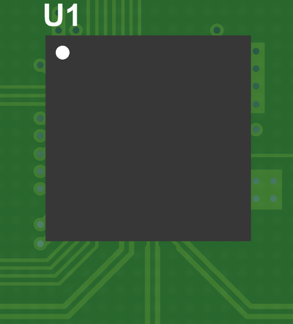
TPS65982BB Top_Placement.pngFigure 24. Top Placement
TPS65982BB Bottom_Placement.pngFigure 25. Bottom Placement