SLVSEZ5A July   2020  – December 2020 TPS25814

PRODUCTION DATA  

  1. Features
  2. Applications
  3. Description
  4. Revision History
  5. Pin Configuration and Functions
  6. Specifications
    1. 6.1  Absolute Maximum Ratings
    2. 6.2  ESD Ratings
    3. 6.3  Recommended Operating Conditions
    4. 6.4  Recommended Capacitance
    5. 6.5  Thermal Information
    6. 6.6  Power Supply Characteristics
    7. 6.7  Power Consumption
    8. 6.8  PP_5V Power Switch Characteristics
    9. 6.9  Power Path Supervisory
    10. 6.10 CC Cable Detection Parameters
    11. 6.11 CC VCONN Parameters
    12. 6.12 Thermal Shutdown Characteristics
    13. 6.13 Input/Output (I/O) Characteristics
    14. 6.14 BC1.2 Characteristics
    15. 6.15 I2C Requirements and Characteristics
    16. 6.16 Typical Characteristics
  7. Parameter Measurement Information
  8. Detailed Description
    1. 8.1 Overview
    2. 8.2 Functional Block Diagram
    3. 8.3 Feature Description
      1. 8.3.1 Power Paths
        1. 8.3.1.1 Internal Sourcing Power Paths
          1. 8.3.1.1.1 PP_5V Current Clamping
          2. 8.3.1.1.2 PP_5V Local Overtemperature Shut Down (OTSD)
          3. 8.3.1.1.3 PP_5V OVP
          4. 8.3.1.1.4 PP_5V UVLO
          5. 8.3.1.1.5 PP_5Vx Reverse Current Protection
          6. 8.3.1.1.6 PP_CABLE Current Clamp
          7. 8.3.1.1.7 PP_CABLE Local Overtemperature Shut Down (OTSD)
          8. 8.3.1.1.8 PP_CABLE UVLO
      2. 8.3.2 Cable Plug and Orientation Detection
        1. 8.3.2.1 Configured as a Source
      3. 8.3.3 Overvoltage Protection (CC1, CC2)
      4. 8.3.4 Default Behavior Configuration (ADCIN1, ADCIN2)
      5. 8.3.5 BC 1.2 (USB_P, USB_N)
      6. 8.3.6 Digital Interfaces
        1. 8.3.6.1 Fault Indicators ( FAULT )
        2. 8.3.6.2 Sink Attachment Indicator ( SINK )
        3. 8.3.6.3 Polarity Indicator ( POL )
        4. 8.3.6.4 Power Management ( CHG_HI)
        5. 8.3.6.5 Battery Charging Control (CTL)
        6. 8.3.6.6 Debug Accessory Detection ( DEBUG)
        7. 8.3.6.7 Disable the Port (EN)
        8. 8.3.6.8 I2C Interface
      7. 8.3.7 I2C Interface
        1. 8.3.7.1 I2C Interface Description
        2. 8.3.7.2 I2C Clock Stretching
        3. 8.3.7.3 I2C Address Setting
        4. 8.3.7.4 Unique Address Interface
    4. 8.4 Device Functional Modes
      1. 8.4.1 Pin Strapping to Configure Default Behavior
      2. 8.4.2 Power States
      3. 8.4.3 Schottky for Current Surge Protection
      4. 8.4.4 Thermal Shutdown
  9. Application and Implementation
    1. 9.1 Application Information
    2. 9.2 Typical Application
      1. 9.2.1 Type C DFP Port Implementation with Embedded Controller
        1. 9.2.1.1 Detailed Design Procedure
          1. 9.2.1.1.1 Type-C Connector VBUS Capacitors
          2. 9.2.1.1.2 VBUS Schottky and TVS Diodes
          3. 9.2.1.1.3 VBUS Snubber Circuit
        2. 9.2.1.2 Application Curves
  10. 10Power Supply Recommendations
    1. 10.1 3.3-V Power
      1. 10.1.1 VIN_3V3 Input Switch
    2. 10.2 1.5-V Power
    3. 10.3 Recommended Supply Load Capacitance
  11. 11Layout
    1. 11.1 Layout Guidelines
      1. 11.1.1 Top TPS25814 Placement and Bottom Component Placement and Layout
    2. 11.2 Layout Example
    3. 11.3 Component Placement
    4. 11.4 Routing and View Placement
  12. 12Device and Documentation Support
    1. 12.1 Device Support
      1. 12.1.1 Third-Party Products Disclaimer
    2. 12.2 Documentation Support
      1. 12.2.1 Related Documentation
    3. 12.3 Support Resources
    4. 12.4 Trademarks
    5. 12.5 Electrostatic Discharge Caution
    6. 12.6 Glossary
  13. 13Mechanical, Packaging, and Orderable Information
VBUS Snubber Circuit
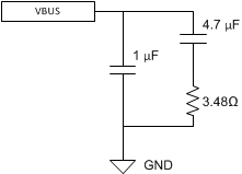
GUID-9924FDBA-014D-46AA-85E7-4C952E5C08B0-low.gif Figure 9-2 VBUS Snubber

Another method of clamping the USB Type-C VBUS is to use a VBUS RC Snubber. An RC Snubber is smaller than a TVS diode, and typically more cost effective as well. An RC Snubber works by modifying the characteristic of the total RLC response in the USB Type-C cable hot-plug from being under-damped to critically-damped or over-damped. So rather than clamping the overvoltage directly, it changes the hot-plug response from under-damped to critically-damped, so the voltage on VBUS does not ring at all; so the voltage is limited, but without requiring a clamping element like a TVS diode.

However, the USB Type-C and Power Delivery specifications limit the range of capacitance that can be used on VBUS for the RC snubber. VBUS capacitance must have a minimum 1 µF and a maximum of 10 µF. The RC snubber values chosen support up to 4 m USB Type-C cable (maximum length allowed in the USB Type-C specification) being hot plugged, is to use 4.7-μF capacitor in series with a 3.48-Ω resistor. In parallel with the RC Snubber a 1-μF capacitor is used, which always ensures the minimum USB Type-C VBUS capacitance specification is met. This circuit is shown in Figure 9-2.