SLVU151A April   2013  – August 2021 TPS54350 , TPS54550


  1.   Trademarks
  2. 1Background
  3. 2Performance Specification Summary
  4. 3Modifications
    1. 3.1 Output Voltage Set Point
    2. 3.2 Input Voltage Range
  5. 4Test Setup and Results
    1. 4.1 Input / Output Connections
    2. 4.2 Efficiency
    3. 4.3 Output Voltage Regulation
    4. 4.4 Load Transients
    5. 4.5 Loop Characteristics
    6. 4.6 Output Voltage Ripple
    7. 4.7 Input Voltage Ripple
    8. 4.8 Powering Up
  6. 5Board Layout
    1. 5.1 Layout
  7. 6Schematic and Bill of Materials
    1. 6.1 Schematic
    2. 6.2 Bill of Materials
  8. 7Revision History

Output Voltage Regulation

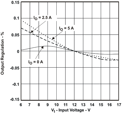
The output voltage load regulation of the TPS54550EVM-158 is shown in Figure 4-2; the output voltage line regulation is shown in Figure 4-3. Measurements are given for an ambient temperature of 25°C.
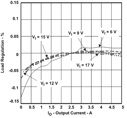
GUID-B84A562E-1B1C-4115-83B2-B4784280129D-low.gifFigure 4-2 Load Regulation
GUID-617CE509-B20F-41A8-8002-FE0674E31B74-low.gifFigure 4-3 Line Regulation