SLVU435A February 2011 – January 2022 TPS53126
- Trademarks
- 1 Introduction
- 2 Electrical Performance Specifications
- 3 Schematic
- 4 Connector and Test Point Descriptions
- 5 Test Setup
- 6 Test Procedure
- 7 Performance Data and Typical Characteristic Curves
- 8 EVM Assembly Drawings and Layout
- 9 Bill of Materials
- 10Revision History
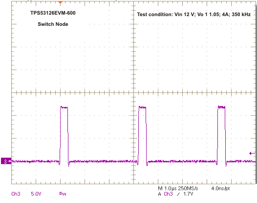
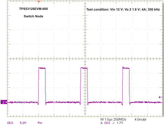
7.4 Switch Node Waveforms
 Figure 7-7 Switching Waveform (VIN = 12 V, VOUT1 = 1.05 V, IOUT1 = 4 A, FSW = 350 kHz)
 Figure 7-8 Switching Waveform (VIN = 12 V, VOUT2 = 1.08 V, IOUT2 = 4 A, FSW = 350 kHz)