SLVUBJ9A July 2020 – October 2020 TPS54JB20
3.3 Layout
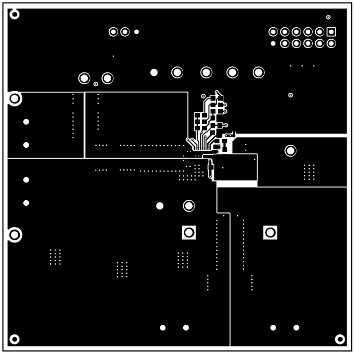
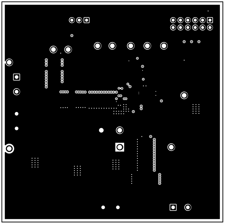
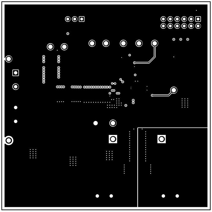
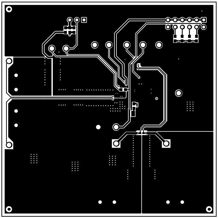
The board layout for the TPS54JB20EVM is shown in Figure 3-2 through Figure 3-5. The top-side layer of the EVM is laid out in a manner typical of a user application. The top, bottom, and internal layers are 2-oz. copper.
The top layer contains the main power traces for VIN, VOUT, and SW. Also on the top layer are connections for the remaining pins of the TPS54JB20 and the majority of the signal traces. The top layer has a dedicated ground plane for quiet analog ground that is connected to the main power ground plane at a single point. The internal layer-1 is a large ground plane. The internal layer-2 contains an additional large ground copper area as well as an additional VOUT copper fill. The bottom layer is another ground plane with two additional traces for the output voltage feedback and various signals routed to test points and headers. There are also additional VIN and VOUT planes on the bottom layer. The top-side ground traces are connected to the bottom and internal ground planes with multiple via groupings placed around the board.
The input decoupling capacitors and bootstrap capacitor are all located as close to the IC as possible. Additionally, the voltage set point resistor divider components are kept close to the IC. The voltage divider network ties to the output voltage at the point of regulation, the copper VOUT trace at the TP4 test point. An additional input bulk capacitor is used to limit the noise entering the converter from the input supply. Critical analog circuits that are noise sensitive are terminated to the quiet analog ground island on the top layer.
 Figure 3-2 TPS54JB20EVM Top-Side Layout
 Figure 3-3 TPS54JB20EVM Internal Layer-1 Layout
 Figure 3-4 TPS54JB20EVM Internal Layer-2 Layout
 Figure 3-5 TPS54JB20EVM Bottom-Side Layout