SLVUBU9A April 2020 – September 2020 TPS63900
- Trademarks
- 1Introduction
-
2Setup
- 2.1
Input/Output Connector and Header Descriptions
- 2.1.1 J1, Pin 1 and 2 – VIN
- 2.1.2 J1, Pin 3 and 4 – S+/S-
- 2.1.3 J1, Pin 5 and 6 – GND
- 2.1.4 J2, Pin 1 and 2 – VOUT
- 2.1.5 J2, Pin 3 and 4 – S+/S-
- 2.1.6 J2, Pin 5 and 6 – GND
- 2.1.7 J4 – GND
- 2.1.8 JP1 – SEL
- 2.1.9 JP2 – ENABLE
- 2.1.10 JP3 – CFG1
- 2.1.11 JP4 – CFG2
- 2.1.12 JP5 – CFG3
- 2.1.13 S1, S2, S3, S4, S5, S6 – IC Configuration (R2D Interface)
- 2.2 Setup
- 2.1
Input/Output Connector and Header Descriptions
- 3Board Layout
- 4Schematic
- 5Bill of Materials
- Revision History
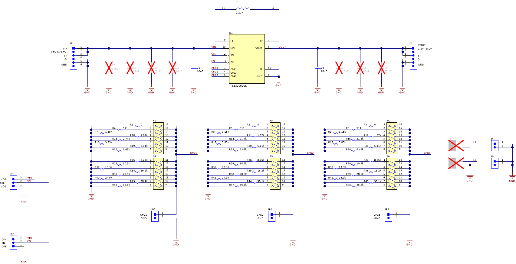
4 Schematic
The red crosses indicate that these components are not populated.
 Figure 4-1 Schematic