SLVUBX0A July   2021  – January 2022 TPSM8A28 , TPSM8A29


  1.   Trademarks
  2. 1Introduction
  3. 2Description
  4. 3Getting Started With the TPSM8A29EVM
    1. 3.1 J1 - Input Voltage Supply Connector
    2. 3.2 J4 and J7 - Positive and Negative Output Connectors
    3. 3.3 J2 - Enable Header
    4. 3.4 J5 - Switching Frequency and Operating Mode
    5. 3.5 J6 - Output Voltage Selection Header
  5. 4Test Point Description
    1. 4.1 TP12 - SS/REF_IN
    2. 4.2 TP14 - VCC
  6. 5Test Setup and Results
    1. 5.1 Startup Procedure
    2. 5.2 Efficiency
    3. 5.3 Load Regulation
    4. 5.4 Line Regulation
    5. 5.5 Output Voltage Ripple
    6. 5.6 Startup and Shutdown
    7. 5.7 Load Transient
    8. 5.8 Bode Plot
  7. 6TPSM8A29EVM Schematic
  8. 7TPSM8A29EVM PCB Layers
  9. 8TPSM8A29EVM Bill of Materials
  10. 9Revision History

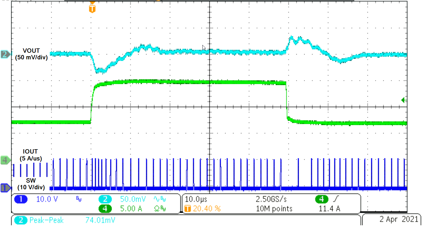
Load Transient

Equation 9. VIN = 12 V, VOUT = 1.0 V, COUT = 8x47 μF
GUID-20210405-CA0I-JRD7-ZRVZ-MRPVZ5PRR1XG-low.png
VIN = 12 V ISTEP = 7.5 A-15 A-7.5 A fsw = 600 kHz Internal bias FCCM
Figure 5-31 Load Transient, 7.5 A step, 10 μs/div, VTRANS = 74 mV