SLVUCG6 November   2022 TPS650350-Q1


  1.   TPS650350-Q1 EVM User's Guide
  2.   Trademarks
  3. Introduction
  4. Requirements
  5. Operation Instructions
    1. 3.1 Configuring the USB to I2C Adapter
    2. 3.2 Regulator Input Supplies and Features
      1. 3.2.1 Buck 1 Input Supply
      2. 3.2.2 Mid-Vin Buck1 Features
      3. 3.2.3 Buck 2/LDO Input Supply
      4. 3.2.4 Buck 3 Input Supply
      5. 3.2.5 Low-Vin Buck2 and Buck3 Features
      6. 3.2.6 Low Noise LDO Features
    3. 3.3 Selecting the Logic Supply Voltage
  6. EVM Configurations
  7. Test Points
    1. 5.1 Voltage Test Points
  8. Graphical User Interface
    1. 6.1 TPS650350-Q1 EVM Debugging
      1. 6.1.1 I2C Communication Port and Adapter Debugging
      2. 6.1.2 Updating MCU Firmware
    2. 6.2 Navigating the GUI
      1. 6.2.1 Home
      2. 6.2.2 Block Diagram
      3. 6.2.3 Registers
      4. 6.2.4 Device Configuration
        1. 6.2.4.1 Using Device Configuration to Define Spin Settings
        2. 6.2.4.2 Configuring the Power Sequence
      5. 6.2.5 Re-Program PMIC
    3. 6.3 In-Circuit Programming
  9. Typical Performance Plots
    1. 7.1 Power Sequence Plots
    2. 7.2 Load Transient Plots
    3. 7.3 Output Voltage Ripple Plots
    4. 7.4 LDO Output Noise
  10. TPS650350-Q1 EVM Schematic
  11. TPS650350-Q1 EVM PCB Layers
  12. 10TPS650350-Q1 EVM Bill of Materials

Home

The Home section is the landing page of the GUI. Here the GUI presents an overview of the compatible EVM and Programming BoosterPack (BOOSTXL-TPS65033), and emphasize navigation to the remaining four sections through the tiles on the bottom of the page.
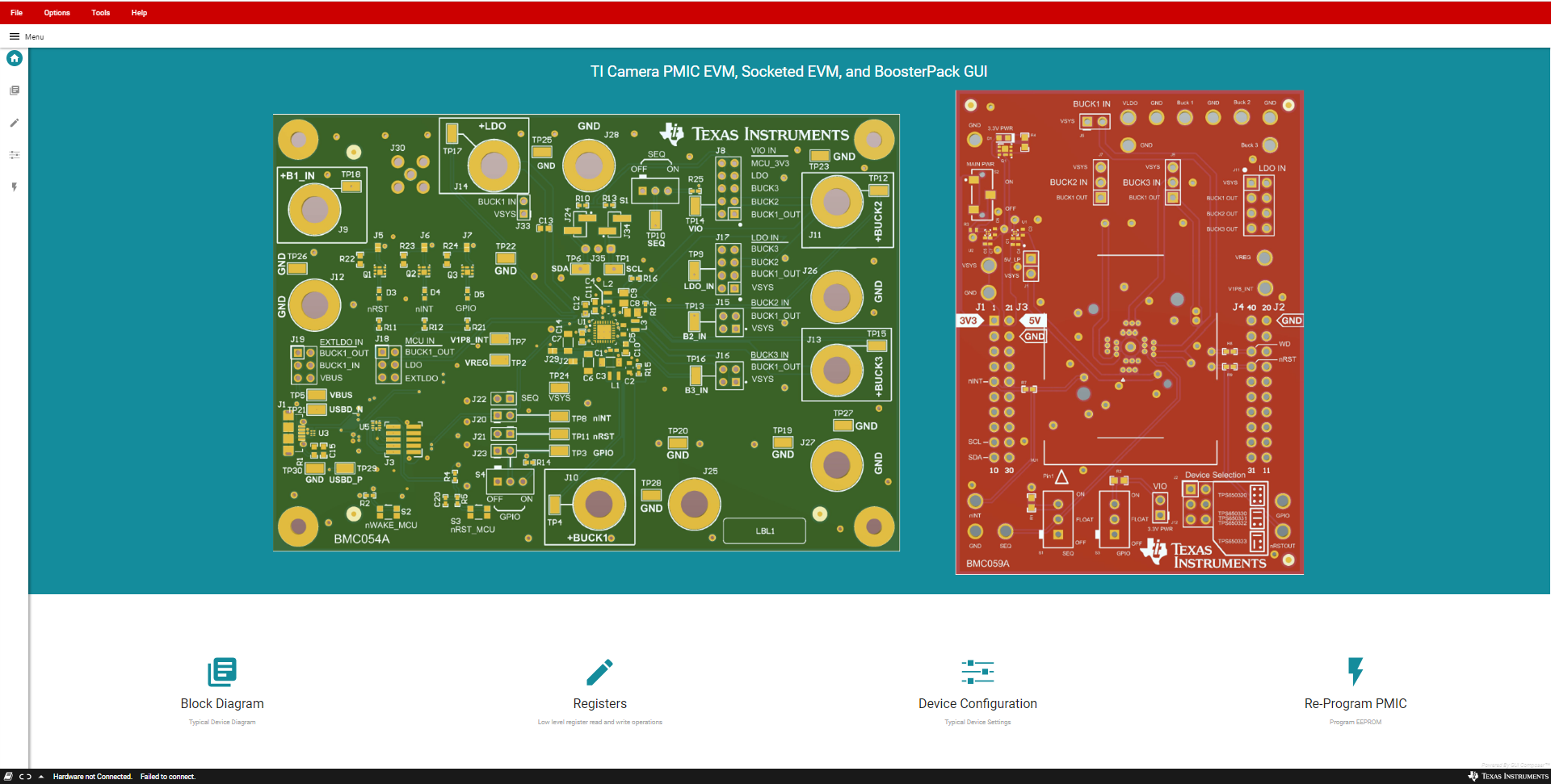
GUID-F477AEAB-7531-432A-8063-E7F85DC1D687-low.pngFigure 6-4 TPS6503xx-Q1 GUI Home Screen