SLVUCG6 November   2022 TPS650350-Q1


  1.   TPS650350-Q1 EVM User's Guide
  2.   Trademarks
  3. Introduction
  4. Requirements
  5. Operation Instructions
    1. 3.1 Configuring the USB to I2C Adapter
    2. 3.2 Regulator Input Supplies and Features
      1. 3.2.1 Buck 1 Input Supply
      2. 3.2.2 Mid-Vin Buck1 Features
      3. 3.2.3 Buck 2/LDO Input Supply
      4. 3.2.4 Buck 3 Input Supply
      5. 3.2.5 Low-Vin Buck2 and Buck3 Features
      6. 3.2.6 Low Noise LDO Features
    3. 3.3 Selecting the Logic Supply Voltage
  6. EVM Configurations
  7. Test Points
    1. 5.1 Voltage Test Points
  8. Graphical User Interface
    1. 6.1 TPS650350-Q1 EVM Debugging
      1. 6.1.1 I2C Communication Port and Adapter Debugging
      2. 6.1.2 Updating MCU Firmware
    2. 6.2 Navigating the GUI
      1. 6.2.1 Home
      2. 6.2.2 Block Diagram
      3. 6.2.3 Registers
      4. 6.2.4 Device Configuration
        1. 6.2.4.1 Using Device Configuration to Define Spin Settings
        2. 6.2.4.2 Configuring the Power Sequence
      5. 6.2.5 Re-Program PMIC
    3. 6.3 In-Circuit Programming
  9. Typical Performance Plots
    1. 7.1 Power Sequence Plots
    2. 7.2 Load Transient Plots
    3. 7.3 Output Voltage Ripple Plots
    4. 7.4 LDO Output Noise
  10. TPS650350-Q1 EVM Schematic
  11. TPS650350-Q1 EVM PCB Layers
  12. 10TPS650350-Q1 EVM Bill of Materials

Configuring the Power Sequence

The Sequencing Overview tab includes instruments to customize the power sequence of the PMIC. Note that the check boxes are power sequence masks. If a particular logic signal needs to be included as part of the regulator or logic power up sequence, leave the box next to the logic signal unchecked. TI recommends to set Power On Bit unmasked for each rail that is required in the application.
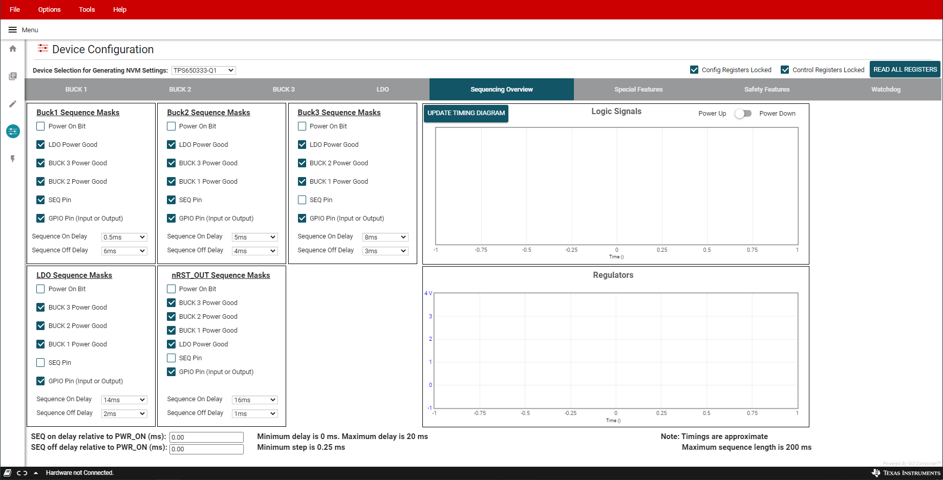
GUID-DD3C70D6-5EF4-43B0-9F36-51B90BF5A9CB-low.pngFigure 6-10 Sequencing Overview Tab
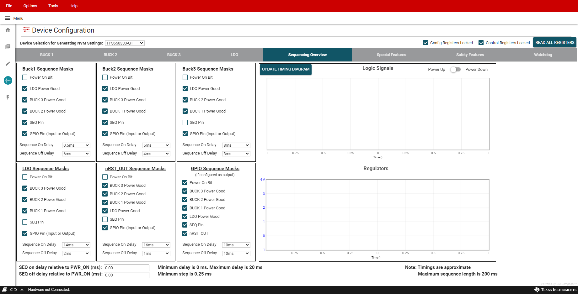
When using a TPS65033x-Q1 device, the GPIO pin can also be used for power sequencing of an external regulator or other device. In the Special Features tab, configure GPIO as an output to include its sequencing in the Sequencing Overview tab. Note that when using GPIO for sequencing, the GPIO Function must be Enabled.
GUID-184E0142-8521-48FE-91AE-702FF08E7B94-low.pngFigure 6-11 Sequencing Overview Including GPIO
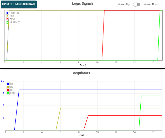
For reference, the GUI can generate example power-up and power-down timing diagrams based on the sequence settings present when the UPDATE TIMING DIAGRAM button is clicked. As noted, rise and fall times are approximate, and the maximum sequence length is 200 ms. Changes to regulator enable and output discharge settings are reflected in the timing diagram. If the sequence settings are not valid, the GUI provides a notifying message and the timing diagram is not updated. For example, if a regulator is enabled but fails to power-up within 200 ms, the sequence settings are not valid.
GUID-DE5C81F4-07E2-4624-9596-57E4360B7BE3-low.pngFigure 6-12 GUI Generated Timing Diagram