SLVUCV2 September 2024 TPS4HC120-Q1
4.2 TPS4HC120-Q1 EVM Assembly Drawings and Layout
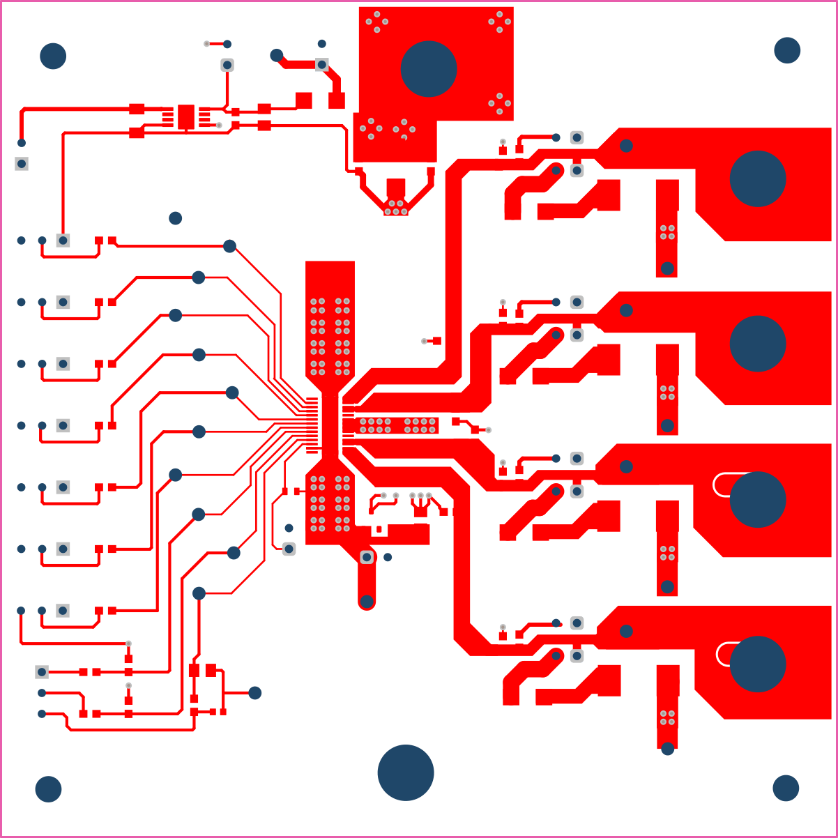
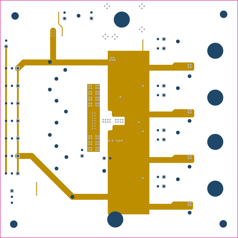
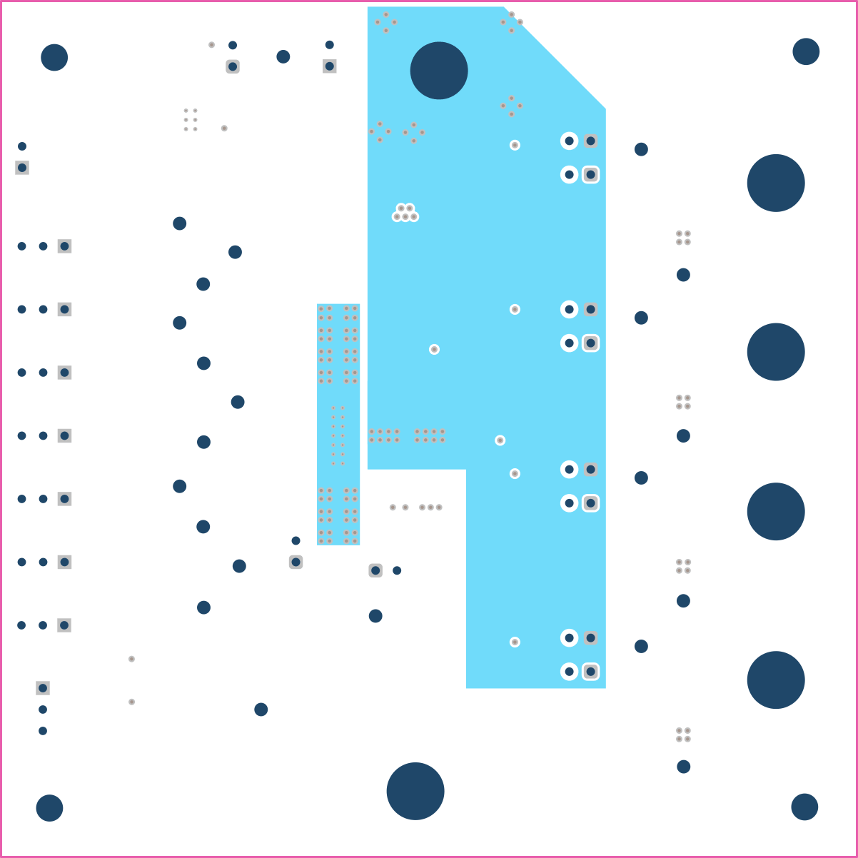
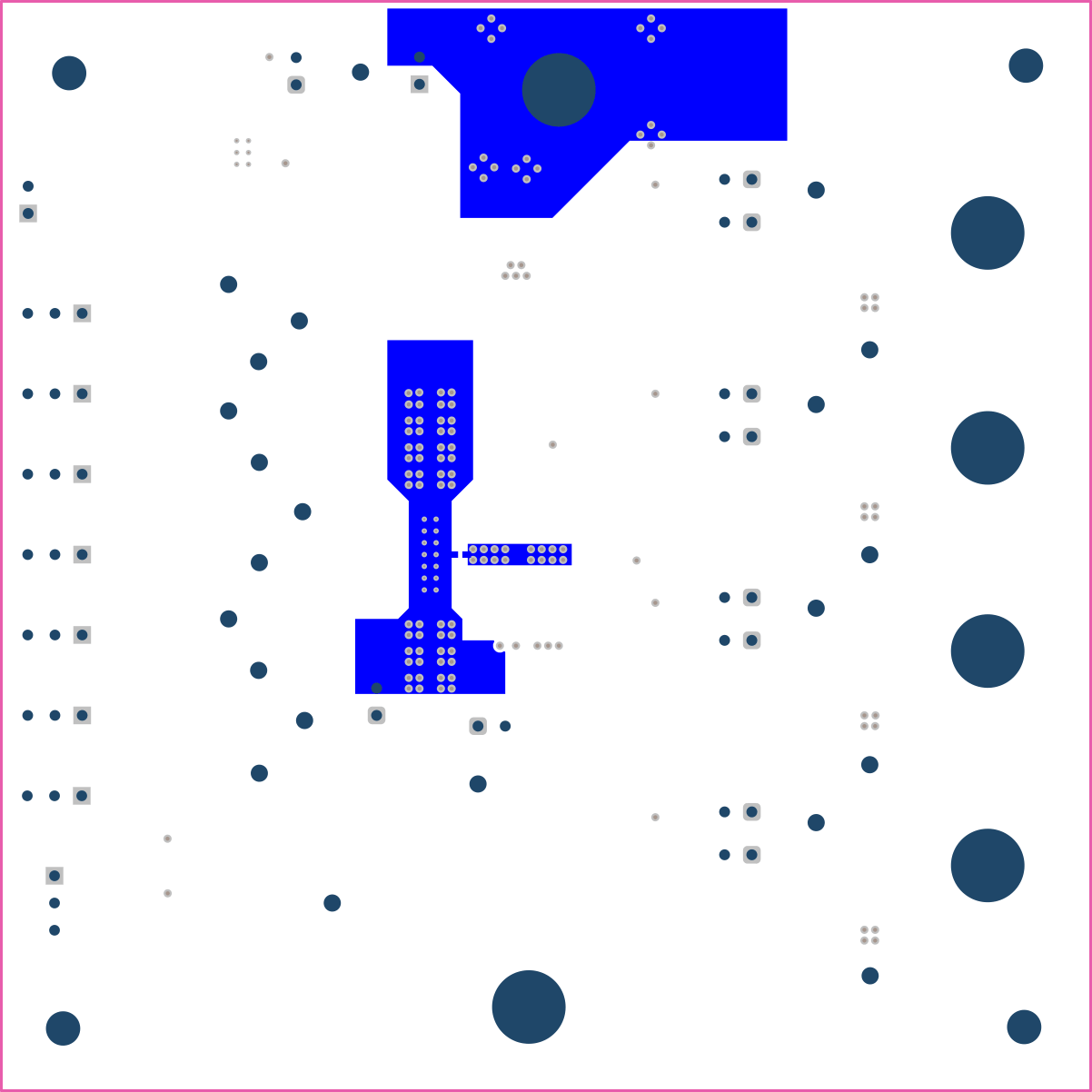
The design of the TPS4HC120-Q1 printed-circuit board (PCB) is shown in Figure 4-2 to Figure 4-5. The EVM is designed using FR4 material, four-layer (2s2p), 2 × 70µm cubic in. top and bottom layers, and 2 × 35µm cubic in. internal plane layers. All components are in an active area on the top side and all active traces to the top and bottom layers to allow the user to easily view, probe, and evaluate. Moving components to both sides of the PCB offers additional size reduction for space-constrained systems.
 Figure 4-2 TPS4HC120-Q1EVM First Layer (Top View)
 Figure 4-3 TPS4HC120-Q1EVM Second Layer GND (Top View)
 Figure 4-4 TPS4HC120-Q1EVM Third Layer VCC (Top View)
 Figure 4-5 TPS4HC120-Q1EVM Fourth Layer (Top View)