SLVUCY2 April 2024 DRV8161
2.2 Faults, Indicators, and Jumper Settings
The DRV8161 implements bootstrap undervoltage, GVDD undervoltage, overcurrent protection, and thermal shutdown in case of overtemperature. See the DRV8161 data sheet for more information on DRV8161 fault support.
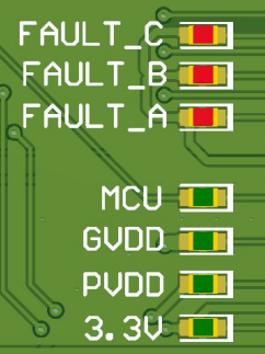
Status LEDs for the MCU, 3.3V, PVDD, GVDD, and FAULT (per phase) are included and shown below.
 Figure 2-6 Status and Fault LEDs
The FAULT LED lights up if the EVM senses a fault. See the data sheet for fault response and corrective actions.
The faults can be reset in the GUI software using the CLEAR FAULTS button. More details on the GUI can be found in Section 3.1.
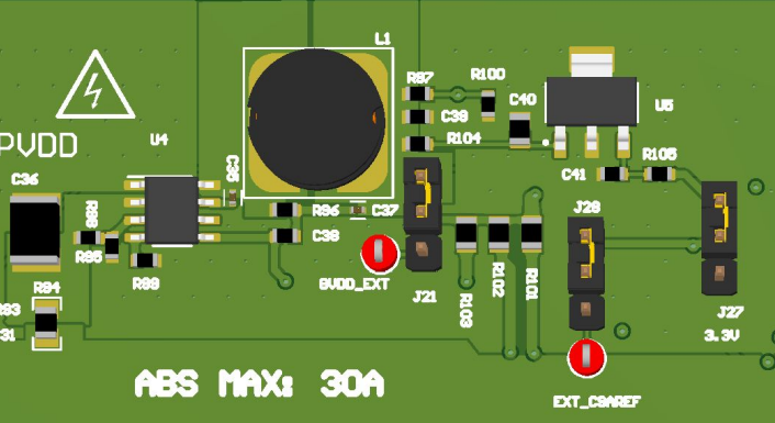
 Figure 2-7 On-Board Buck and LDO
The EVM includes a buck regulator to generate a 12V GVDD Buck voltage from PVDD supply. If external GVDD is needed, then move the J21 jumper to the bottom position.
The GVDD voltage is used to generate 3.3V LDO output. If external 3.3V is needed, then move the J27 jumper to the bottom position. The 3.3V LDO is used to generate the CSAREF voltage. This LaunchPad and EVM works with the 3.3V only. If external voltage is needed, then move the J28 Jumper to the bottom position. (Note this can require board modifications.)
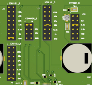
 Figure 2-8 Driver Hardware
Settings
Figure 2-8 Driver Hardware
SettingsThe hardware settings of the DRV8161 can be set as shown in Table 2-1. For more information on resistor to settings, please consult the data sheet.
| Setting | Phase A | Phase B | Phase C |
|---|---|---|---|
| IDRIVE 1 | J1 | J6 | J11 |
| IDRIVE 2 | J4 | J9 | J14 |
| CSAGAIN | J3 | J8 | J13 |
| VDSLVL | J2 | J7 | J12 |
| DTMODE | J5 | J10 | J15 |