SLYT793A may 2020 – may 2020 LM61460-Q1
- 1
- 1 Introduction
- 2 Managing Thermals with Flip-chip Packages
- 3 Board Construction Influence
- 4 Copper Area and Thermals
- 5 Estimating a Converter’s Junction Temperature
- 6 Challenges with Measuring Converter Junction Temperature
- 7 Further Thermal Optimization at the IC Level
- 8 Conclusion
- 9 References
- 10Related Web Sites
2 Managing Thermals with Flip-chip Packages
No matter how efficient a buck converter is, losses will occur in the power stage. Power converter losses cause the device junction temperature to rise and prevent safe operation at higher ambient temperatures. Converter design for high ambient temperatures requires proper thermal management to ensure that the converter’s recommended maximum rated junction temperature is not exceeded, and to prevent the converter from heating up neighboring devices.
 Figure 1 Reduced Solution Area with the
LM61440-Q1 Buck Converter
Figure 1 Reduced Solution Area with the
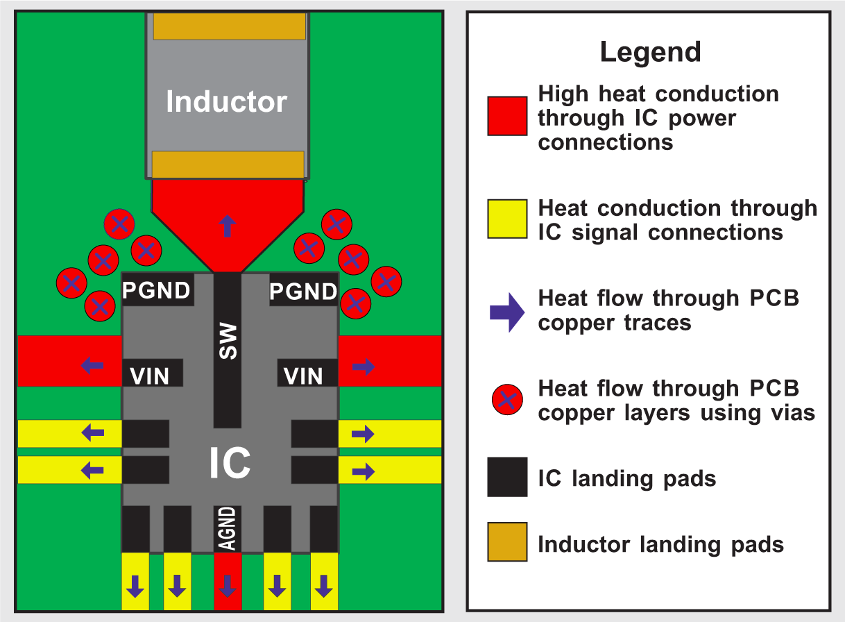
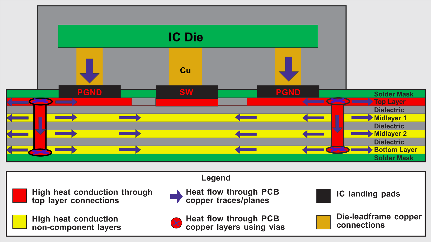
LM61440-Q1 Buck ConverterMany semiconductor manufacturers are implementing converters in a flip-chip package design. A flip-chip device often has a quad flat no-lead (QFN) package, with low-inductance connections made from the semiconductor die to the leadframe. This strikes a good balance between thermal and noise performance. However, the package may lack a thermal pad on its bottom side, which reduces its thermal effectiveness. Nevertheless, with flip-chip devices, efficient heat conduction can occur through the die-to-leadframe copper connections (Figure 2 and Figure 3).
To avoid excessive temperature rise, it makes sense to provide a high thermal conductivity path from the landing pad away from the device. Wide traces to the device landing pads can allow for heat dissipation in the component layer. Dense PCB layouts prevent effective heat dissipation in the component layer, especially with inefficient (hot) neighboring devices. As shown in Figure 3, heat sinking in the inner layers is often more effective than heat dissipation in the component layers. Connecting thermal vias to copper that is connected to the device power or return pins will achieve heat sinking. These vias will then connect to copper planes underneath the IC, increasing the effective copper area for heat sinking. It’s important to place the vias in a way that minimizes thermal bottlenecks, while providing the highest via count with the lowest thermal resistivity to power pins (Figure 2).
 Figure 2 Top View of Flip-chip
Die-to-package Heat-conduction Path for PCB Layer Heat Sinking
 Figure 3 Board Layer View of Flip-chip
Die-to-package Heat-conduction Paths