SNAU182A March   2021  – May 2022


  1.   Trademarks
  2. 1LMX2571EPEVM Evaluation Module
    1. 1.1 Evaluation Module Contents
    2. 1.2 Evaluation Setup Requirement
    3. 1.3 Resources
  3. 2Setup
    1. 2.1 Connection Diagram
    2. 2.2 Power Supply
    3. 2.3 Reference Clock
    4. 2.4 RF Output
    5. 2.5 Programming
    6. 2.6 Evaluation Software
    7. 2.7 EVM Strap Options
      1. 2.7.1 J11 Header
      2. 2.7.2 J12 Header
  4. 3Typical Measurement
    1. 3.1 Default Configuration
      1. 3.1.1 Loop Filter
      2. 3.1.2 Typical Output
    2. 3.2 Additional Tests
      1. 3.2.1 FSK Modulation
      2. 3.2.2 Register Readback
  5. 4Schematic
  6. 5Board Construction
    1. 5.1 PCB Layer Stack-Up
    2. 5.2 PCB Layout
  7. 6Bill of Materials
  8. 7Troubleshooting Guide
  9.   A Using Different Reference Clock
  10.   B Reference PRO
    1.     B.1 Output Frequency Selection
    2.     B.2 Output Format Selection
    3.     B.3 Typical Output Characteristics
    4.     B.4 Firmware Update
  11.   C Revision History

Troubleshooting Guide

If the EVM does not work as expected, use the Figure 7-1 to identify potential root causes. Consider the following:

  • Do not make modifications to the EVM or change the default settings until AFTER it is verified to be working.
  • Register read back requires the correct software setup, See Section 3.2.2 for details.
  • The POR current of the LMX2571EPEVM is approximately 30 mA.
  • The power-down current of the LMX2571EPEVM is approximately 3 mA.
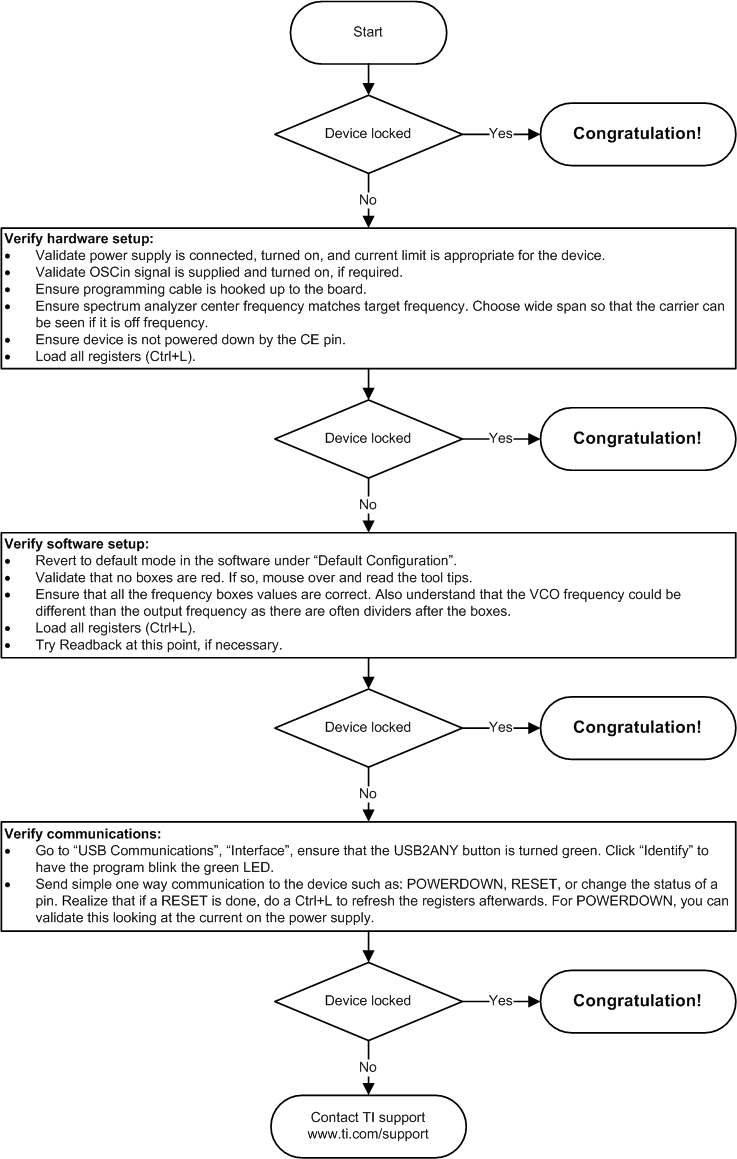
GUID-FE9670ED-718F-4E47-A96F-E1F1CDD4F6AB-low.gif Figure 7-1 Troubleshooting Guide