SNAU296 December 2023 LMK5C33414A
- 1
- Abstract
- Trademarks
- 1Introduction
- 2EVM Quick Start
- 3EVM Configuration
-
4EVM
Schematics
- 4.1 Power Supply Schematic
- 4.2 Alternative Power Supply Schematic
- 4.3 Power Distribution Schematic
- 4.4 LMK5C33414A and Input References IN0 to IN3 Schematic
- 4.5 Clock Outputs OUT0 to OUT3 Schematic
- 4.6 Clock Outputs OUT4 to OUT9 Schematic
- 4.7 Clock Outputs OUT10 to OUT13 and Clock Inputs IN2 and IN3 Schematic
- 4.8 XO Schematic
- 4.9 Logic I/O Interfaces Schematic
- 4.10 USB2ANY Schematic
- 5EVM Bill of Materials
-
6Appendix A - TICS Pro LMK5C33414A Software
- 6.1 Using the Start Page
- 6.2 Using the Status Page
- 6.3 Using the Input Page
- 6.4 Using APLL1, APLL2, and APLL3 Pages
- 6.5 Using the DPLL1, DPLL2, and DPLL3 Pages
- 6.6 Using the Validation Page
- 6.7 Using the GPIO Page
- 6.8 SYNC/SYSREF/1-PPS Page
- 6.9 Using the Outputs Page
- 6.10 EEPROM Page
- 6.11 Design Report Page
6.9 Using the Outputs Page
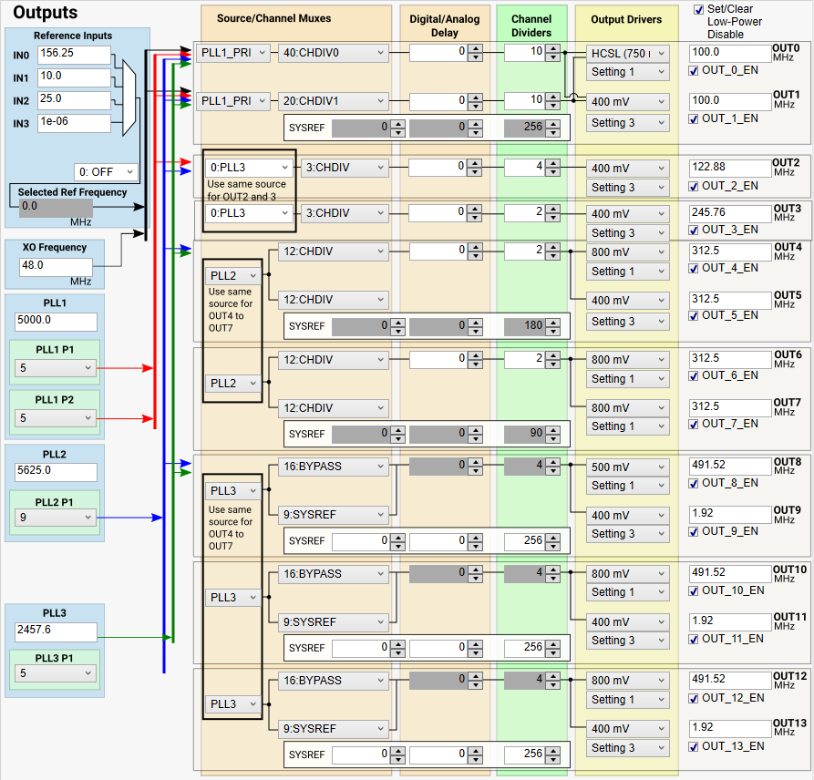
The Outputs page shows all the possible source frequencies to the output channels. To simplify settings fields necessary to providing an output frequency, a source mux lists all possible sources for each output. Be sure to enable or disable the desired outputs on the right-hand side of the screen.
There are many detailed output pages beneath the Outputs page that show the individual controls for each set of outputs.
The black box around OUT2 to OUT3, OUT4 to OUT7, and OUT8 to OUT13 signifies that all these outputs needs to be sourced from the same VCO.
 Figure 6-22 Outputs Page