SNAU310 June   2024 LMKDB1102 , LMKDB1202


  1.   1
  2.   Description
  3.   Features
  4.   Applications
  5.   5
  6. 1Evaluation Module Overview
    1. 1.1 Introduction
    2. 1.2 Kit Contents
    3. 1.3 Specification
    4. 1.4 Device Information
  7. 2EVM Quick Start
    1. 2.1 Setup
    2. 2.2 EVM Measurements
  8. 3Hardware
    1. 3.1 EVM Configuration
      1. 3.1.1 Power Supply
      2. 3.1.2 Logic Input and Outputs
      3. 3.1.3 Clock Input
      4. 3.1.4 Clock Outputs
      5. 3.1.5 Status Outputs, LEDs, and Test Points
  9. 4Implementation Results
    1. 4.1 Typical Phase Noise Characteristic
  10. 5Hardware Design Files
    1. 5.1 Schematics
    2. 5.2 PCB Layouts
    3. 5.3 LMKDB1102EVM Bill of Materials (BOM)
    4. 5.4 LMKDB1202EVM Bill of Materials (BOM)
  11. 6Compliance Information
    1. 6.1 Compliance and Certifications
  12. 7Additional Information
    1. 7.1 Trademarks
  13. 8References

Schematics

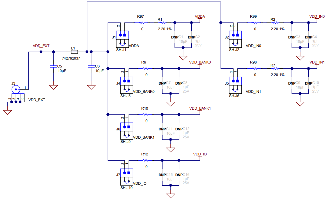
LMKDB1102EVM, LMKDB1202EVM Power Supply Figure 5-1 Power Supply
LMKDB1102EVM, LMKDB1202EVM LMKDB1102 Device and CLKIN0_P/N
          Reference Figure 5-2 LMKDB1102 Device and CLKIN0_P/N Reference
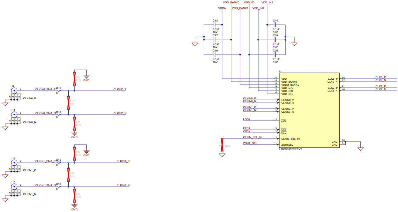
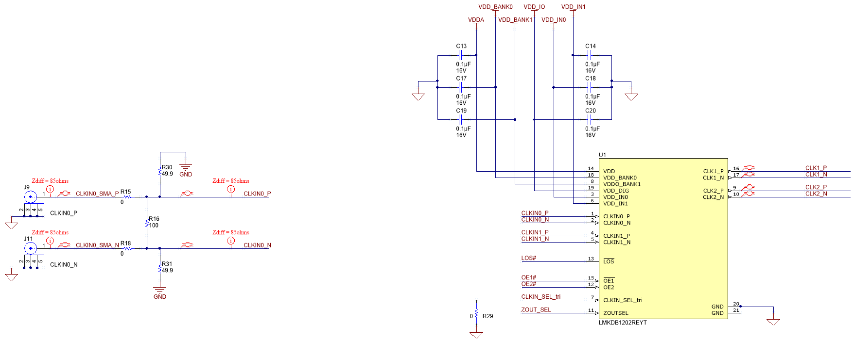
LMKDB1102EVM, LMKDB1202EVM LMKDB1202 Device and CLKIN#_P/N Reference Figure 5-3 LMKDB1202 Device and CLKIN#_P/N Reference
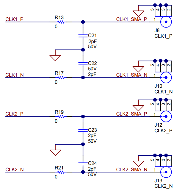
LMKDB1102EVM, LMKDB1202EVM Clock Outputs CLK1 and CLK2 Figure 5-4 Clock Outputs CLK1 and CLK2
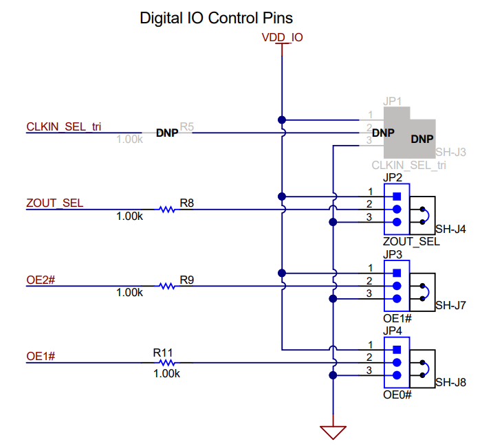
LMKDB1102EVM, LMKDB1202EVM Output Enable Pins (OE#) and LMKDB1102
          Logic I/O Jumpers Figure 5-5 Output Enable Pins (OE#) and LMKDB1102 Logic I/O Jumpers
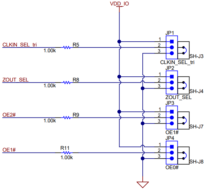
LMKDB1102EVM, LMKDB1202EVM Output Enable Pins (OE#) and LMKDB1202
          Logic I/O Jumpers Figure 5-6 Output Enable Pins (OE#) and LMKDB1202 Logic I/O Jumpers
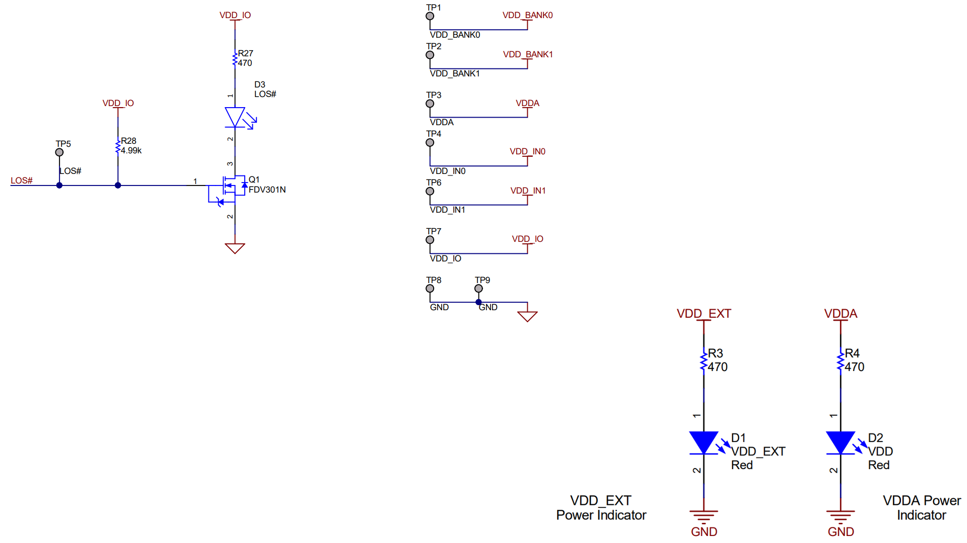
LMKDB1102EVM, LMKDB1202EVM Status LEDs and Test Points Figure 5-7 Status LEDs and Test Points