SNIS187A March 2015 – July 2015 LMT70 , LMT70A
PRODUCTION DATA.
- 1 Features
- 2 Applications
- 3 Description
- 4 Wide-Range Precision Active RTD or NTC Replacement (−55°C to 150°C)
- 5 Revision History
- 6 Device Comparison Table
- 7 Pin Configuration and Functions
- 8 Specifications
- 9 Detailed Description
- 10Application and Implementation
- 11Power Supply Recommendations
- 12Layout
- 13Device and Documentation Support
- 14Mechanical, Packaging, and Orderable Information
10 Application and Implementation
NOTE
Information in the following applications sections is not part of the TI component specification, and TI does not warrant its accuracy or completeness. TI’s customers are responsible for determining suitability of components for their purposes. Customers should validate and test their design implementation to confirm system functionality.
10.1 Application Information
The LMT70 analog output temperature sensor is an ideal device to connect to an integrated 12-Bit ADC such as that found in the MSP430 microcontroller family.
Applications for the LMT70 included but are not limited to: IoT based temperature sensor nodes, medical fitness equipment (e.g. thermometers, fitness/smart bands or watches, activity monitors, human body temperature monitor), Class AA or lower RTD replacement, precision NTC or PTC thermistor replacement, instrumentation temperature compensation, metering temperature compensation (e. g. heat cost allocator, heat meter).
10.2 Typical Application
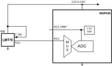 Figure 26. Typical Application Schematic
Most CMOS ADCs found in microcontrollers and ASICs have a sampled data comparator input structure. When the ADC charges the sampling cap, it requires instantaneous charge from the output of the analog source such as the LMT70 temperature sensor and many op amps. This requirement is easily accommodated by the addition of a capacitor (CFILTER) or the extension of the ADC acquisition time thus slowing the ADC sampling rate. The size of CFILTER depends on the size of the sampling capacitor and the sampling frequency. Since not all ADCs have identical input stages, the charge requirements will vary. The general ADC application shown in Figure 27 is an example only. The application in Figure 26 was actually tried and the extension of the MSP430 12-Bit ADC acquisition time was all that was necessary in order to accommodate the LMT70's output stage drive capability.
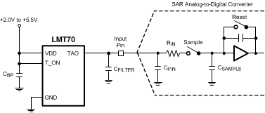 Figure 27. Suggested Connection to a Sampling Analog-to-Digital Converter Input Stage
10.2.1 Design Requirements
The circuit show in Figure 26 will support the design requirements as shown in Table 3.
Table 3. Design Requirements
| PARAMETER | TARGET SPECIFICATION |
|---|---|
| Temperature Range | -40°C to +150°C LMT70, -40°C to +85°C for MSP430 |
| Accuracy | ±0.2°C typical over full temperature range |
| VDD | 2.2V to 3.6V with typical of 3.0V |
| IDD | 12µA |
10.2.2 Detailed Design Procedure
10.2.2.1 Temperature Algorithm Selection
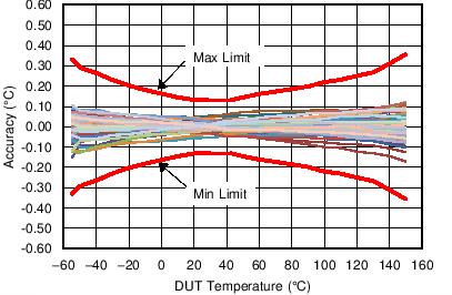
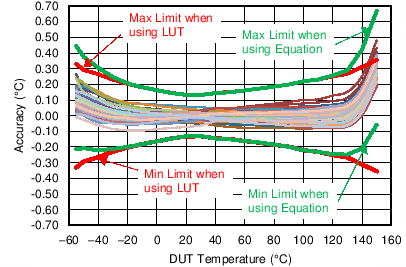
Of the three algorithms presented in this datasheet, linear interpolation, second order transfer function or third order transfer function, the one selected will be determined by the users microcontroller resources and the temperature range that will be sensed. Therefore, a comparison of the expected accuracy from the LMT70 is given here. The following curves show effect on the accuracy of the LMT70 when using each of the different algorithms/equations given in LMT70 Output Transfer Function. The first curve (Figure 28) shows the performance when using linear interpolation of the LUT values shown in Electrical Characteristics Temperature Lookup Table (LUT) of every 10°C and provides the best performance. Linear interpolation of the LUT values shown in Electrical Characteristics Temperature Lookup Table (LUT) is used to determine the LMT70 min/max accuracy limits as shown in the Electrical Characteristics and the red lines of Figure 28. The other lines in the middle of Figure 28 show independent device performance. The green limit lines, shown in the subsequent figures, apply for the specific equation used to convert the output voltage of the LMT70 to temperature. The equations are shown under each figure for reference purposes. The green lines show the min/max limits when set in a similar manner to the red limit lines of Figure 28. The limits shown in red for Figure 28 are repeated in all the figures of this section for comparison purposes.
| Temp (°C) |
VTAO (mV) | Local Slope (mV/°C) |
||
|---|---|---|---|---|
| MIN | TYP | MAX | ||
| 20 | 994.367 | 995.050 | 995.734 | -5.171 |
| 30 | 942.547 | 943.227 | 943.907 | -5.194 |
| 40 | 890.423 | 891.178 | 891.934 | -5.217 |
| 50 | 838.097 | 838.882 | 839.668 | -5.241 |
| TM = -1.809628E-09 (VTAO)3 – 3.325395E-06 (VTAO)2 – 1.814103E-01(VTAO) + 2.055894E+02 |
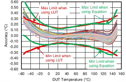
| TM = -7.857923E-06 (VTAO)2 – 1.777501E-01 (VTAO) + 2.046398E+02 |
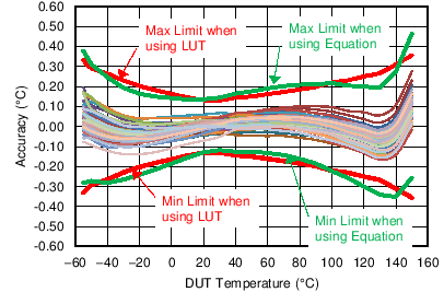
| TM = -1.064200E-09 (VTAO)3 – 5.759725E-06 (VTAO)2 – 1.789883E-01(VTAO) + 2.048570E+02 | ||
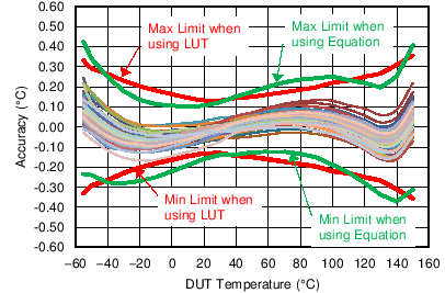
| TM = -8.451576E-06 (VTAO)2– 1.769281E-01 (VTAO) + 2.043937E+02 |
10.2.2.2 ADC Requirements
The ADC resolution and its specifications as well as reference voltage and its specifications will determine the overall system accuracy that you can obtain. For this example the 12-bit SAR ADC found in the MSP430 was used as well as it's integrated reference. At first glance the specifications may not seem to be precise enough to actually be used with the LMT70 but the MSP430 ADC and integrated reference errors are actually measured during production testing of the MSP430. Values are then provided to user for software calibration. These calibration values are located in the MSP430A device descriptor tag-length-value (TLV) structure and found in the device-specific datasheet. The MSP430 Users Guide includes information on how to use these calibration values to calibrate the ADC reading. The specific values used to calibrate the ADC readings are: CAL_ADC_15VREF_FACTOR, CAL_ADC_GAIN_FACTOR and CAL_ADC_OFFSET.
10.2.3 Finer Resolution LUT
The following table is given for reference only and not meant to be used for calculation purposes.
| Temp (°C) |
VTAO
(mV) |
Temp (°C) |
VTAO
(mV) |
Temp (°C) |
VTAO
(mV) |
Temp (°C) |
VTAO
(mV) |
Temp (°C) |
VTAO
(mV) |
Temp (°C) |
VTAO
(mV) |
Temp (°C) |
VTAO
(mV) |
Temp (°C) |
VTAO
(mV) |
|||||||
| TYP | TYP | TYP | TYP | TYP | TYP | TYP | TYP | |||||||||||||||
| -30 | 1250.398 | 0 | 1097.987 | 30 | 943.227 | 60 | 786.360 | 90 | 627.490 | 120 | 466.760 | 150 | 302.785 | |||||||||
| -29 | 1244.953 | 1 | 1092.532 | 31 | 937.729 | 61 | 780.807 | 91 | 621.896 | 121 | 460.936 | |||||||||||
| -28 | 1239.970 | 2 | 1087.453 | 32 | 932.576 | 62 | 775.580 | 92 | 616.603 | 122 | 455.612 | |||||||||||
| -27 | 1234.981 | 3 | 1082.370 | 33 | 927.418 | 63 | 770.348 | 93 | 611.306 | 123 | 450.280 | |||||||||||
| -26 | 1229.986 | 4 | 1077.282 | 34 | 922.255 | 64 | 765.113 | 94 | 606.006 | 124 | 444.941 | |||||||||||
| -55 | 1375.219 | -25 | 1224.984 | 5 | 1072.189 | 35 | 917.087 | 65 | 759.873 | 95 | 600.701 | 125 | 439.593 | |||||||||
| -54 | 1370.215 | -24 | 1219.977 | 6 | 1067.090 | 36 | 911.915 | 66 | 754.628 | 96 | 595.392 | 126 | 434.238 | |||||||||
| -53 | 1365.283 | -23 | 1214.963 | 7 | 1061.987 | 37 | 906.738 | 67 | 749.380 | 97 | 590.079 | 127 | 428.875 | |||||||||
| -52 | 1360.342 | -22 | 1209.943 | 8 | 1056.879 | 38 | 901.556 | 68 | 744.127 | 98 | 584.762 | 128 | 423.504 | |||||||||
| -51 | 1355.395 | -21 | 1204.916 | 9 | 1051.765 | 39 | 896.370 | 69 | 738.870 | 99 | 579.442 | 129 | 418.125 | |||||||||
| -50 | 1350.441 | -20 | 1199.884 | 10 | 1046.647 | 40 | 891.178 | 70 | 733.608 | 100 | 574.117 | 130 | 412.739 | |||||||||
| -49 | 1345.159 | -19 | 1194.425 | 11 | 1041.166 | 41 | 885.645 | 71 | 728.055 | 101 | 568.504 | 131 | 406.483 | |||||||||
| -48 | 1340.229 | -18 | 1189.410 | 12 | 1036.062 | 42 | 880.468 | 72 | 722.804 | 102 | 563.192 | 132 | 401.169 | |||||||||
| -47 | 1335.293 | -17 | 1184.388 | 13 | 1030.952 | 43 | 875.287 | 73 | 717.550 | 103 | 557.877 | 133 | 395.841 | |||||||||
| -46 | 1330.352 | -16 | 1179.361 | 14 | 1025.838 | 44 | 870.100 | 74 | 712.292 | 104 | 552.557 | 134 | 390.499 | |||||||||
| -45 | 1325.405 | -15 | 1174.327 | 15 | 1020.720 | 45 | 864.909 | 75 | 707.029 | 105 | 547.233 | 135 | 385.144 | |||||||||
| -44 | 1320.453 | -14 | 1169.288 | 16 | 1015.596 | 46 | 859.713 | 76 | 701.762 | 106 | 541.905 | 136 | 379.775 | |||||||||
| -43 | 1315.496 | -13 | 1164.242 | 17 | 1010.467 | 47 | 854.513 | 77 | 696.491 | 107 | 536.573 | 137 | 374.393 | |||||||||
| -42 | 1310.534 | -12 | 1159.191 | 18 | 1005.333 | 48 | 849.307 | 78 | 691.217 | 108 | 531.236 | 138 | 368.997 | |||||||||
| -41 | 1305.566 | -11 | 1154.134 | 19 | 1000.194 | 49 | 844.097 | 79 | 685.937 | 109 | 525.895 | 139 | 363.587 | |||||||||
| -40 | 1300.593 | -10 | 1149.070 | 20 | 995.050 | 50 | 838.882 | 80 | 680.654 | 110 | 520.551 | 140 | 358.164 | |||||||||
| -39 | 1295.147 | -9 | 1143.654 | 21 | 989.583 | 51 | 833.343 | 81 | 675.073 | 111 | 514.886 | 141 | 351.937 | |||||||||
| -38 | 1290.202 | -8 | 1138.599 | 22 | 984.450 | 52 | 828.141 | 82 | 669.803 | 112 | 509.557 | 142 | 346.508 | |||||||||
| -37 | 1285.250 | -7 | 1133.540 | 23 | 979.313 | 53 | 822.934 | 83 | 664.528 | 113 | 504.223 | 143 | 341.071 | |||||||||
| -36 | 1280.291 | -6 | 1128.476 | 24 | 974.171 | 54 | 817.723 | 84 | 659.250 | 114 | 498.885 | 144 | 335.625 | |||||||||
| -35 | 1275.326 | -5 | 1123.407 | 25 | 969.025 | 55 | 812.507 | 85 | 653.967 | 115 | 493.542 | 145 | 330.172 | |||||||||
| -34 | 1270.353 | -4 | 1118.333 | 26 | 963.875 | 56 | 807.287 | 86 | 648.680 | 116 | 488.195 | 146 | 324.711 | |||||||||
| -33 | 1265.375 | -3 | 1113.254 | 27 | 958.720 | 57 | 802.062 | 87 | 643.389 | 117 | 482.843 | 147 | 319.241 | |||||||||
| -32 | 1260.389 | -2 | 1108.170 | 28 | 953.560 | 58 | 796.832 | 88 | 638.094 | 118 | 477.486 | 148 | 313.764 | |||||||||
| -31 | 1255.397 | -1 | 1103.081 | 29 | 948.396 | 59 | 791.598 | 89 | 632.794 | 119 | 472.125 | 149 | 308.279 |
10.2.4 Application Curves
The LMT70 performance using the MSP430 with integrated 12-bit ADC is shown in Figure 33. This curve includes the error of the MSP430 integrated 12-bit ADC and reference as shown in the schematic Figure 26. The MSP430 was kept at room temperature and the LMT70 was submerged in a precision temperature calibration oil bath. A calibrated temperature probe was used to monitor the temperature of the oil. As can be seen in Figure 33 the combined performance on the MSP430 and the LMT70 is better than 0.12°C for the entire -40°C to +150°C temperature range. The only calibration performed was with software using the MSP430A device descriptor tag-length-value (TLV) calibration values for ADC and VREF error.
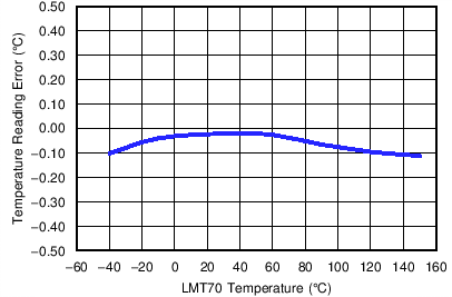 Figure 33. LMT70 with MSP430 typical performance
10.3 System Examples
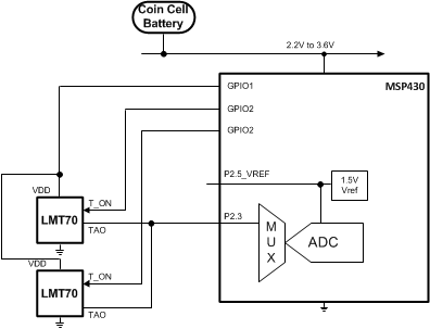 Figure 34. Multiple LMT70s connected to one 12-bit ADC channel on an MSP430
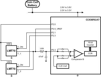 Figure 35. Multiple LMT70s connected to a slope ADC for high resolution