SNLU343 June 2024 DP83TD510E
2.2 Header Information
This EVM consists of two boards: one is the power sourcing equipment (PSE) and one is the powered device (PD).
Power Sourcing Equipment (PSE)
 Figure 2-4 PSE Block Diagram
Figure 3-4 shows the block diagram of the PSE board. The board is divided in four sub blocks, the power supply, the PSE circuit, the media converter, and the USB2MDIO interface. For implementation details, refer to the schematic and related documentation.
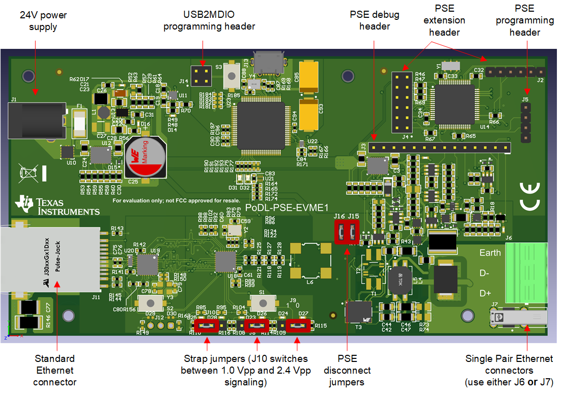
 Figure 2-5 PSE Jumpers
All jumpers and headers are shown in Figure 3-5. The default settings are shown in the figure. Jumper J10 can be used to switch the SPE PHY between 1.0 Vpp signaling and 2.4 Vpp signaling. The default settings configure the PHY for 2.4 Vpp.
Two jumpers, J15 and J16, are allowed to disconnect the PSE stage from the coupling network. This allows to either use the PSE block in combination with a coupling network or to use an own PSE implementation with the onboard SPE PHY and coupling network. Also, these jumpers are a good point to probe the behavior of the PSE block without interfering with the data signal.
The USB2MDIO and PSE digital block have a microcontroller and are pre-programmed. Refer to the images below for the correct pinout of the programming headers if an update or change of the firmware is needed.
 Figure 2-6 Programming header
USB2MDIO
 Figure 2-7 Programming Header PSE
The signals between the PSE digital part and analog parts are brought out on a connector for easy probing. This helps in case of problems to investigate what is happening. Figure 3-8 shows the pinout of this connector.
 Figure 2-8 Debug header PSE
The table below details the signals present on the PSE debug header.
| Signal | Description | Normal operation, PD connected and powered |
|---|---|---|
|
Imon |
Output from eFuse, outputs a voltage proportional to connected load |
0 - 3 V |
|
Iset |
Input to eFuse to set current limit with a voltage |
0 - 1 V |
|
!Fault |
Fault output from eFuse |
3.3 V |
|
!SHDN |
Disabled output of eFuse |
3.3 V |
|
SCCP_DOUT |
Output from MCU to send SCCP data |
0 V, communication before power up |
|
SCCP_DIN |
Input to MCU for reading SCCP data |
3.3 V, communication before power up |
|
VID_valid |
Signals a valid detection voltage |
0 V, short pulse before power up |
|
!CS_on |
Enables current source for detection and classification |
0 V, short pulse before power up |
|
MVFS_valid |
Signals current flow to MCU |
3.3 V |
|
Prebias_ok |
Signals valid prebias current |
0 V, short pulse before power up |
|
Prebias_en |
Enables prebias/sleep voltage source |
0 V, short pulse before power up |
If the user wants to modify the firmware of the PSE controller, then there are additional pins of the microcontroller brought out for extensions, such as an additional PSE port. Figure 3-9 shows the pinout.
 Figure 2-9 Extension Header PSE
Powered Device (PD)
 Figure 2-10 PD Block Diagram
Figure 3-10 shows how the power device is built up. The block diagram consists of similar blocks as the PSE, but includes a modified power supply and replaces the PSE by a PD block.
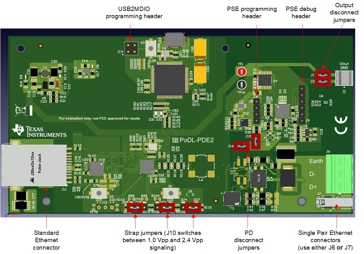
 Figure 2-11 PD Jumpers
For the jumper settings, refer to Figure 3-11. Similarly as the PSE side, follow the settings shown. J10 can be used to select 1.0 Vpp instead of 2.4 Vpp. The jumpers J15 and J16 can be used to separate the PD from the coupling network. The jumpers J1 and J3 allow to disconnect the Vout connector and allows adding an isolated power supply instead of the jumpers.
Additionally, the microcontrollers involved, so there are programming headers as well. The USB 2 MDIO programming header is exactly the same as for the board mentioned before. The pinout for the PD controller header is shown in Figure 3-12.
 Figure 2-12 Programming Header PD
The PD board allows access to the SCCP signals for debugging purpose. The pinout of the connector is shown in Figure 3-13.
 Figure 2-13 Debug Header PD