SNOA961A February   2017  – February 2023 LDC2112 , LDC2114 , LDC3114 , LDC3114-Q1


  1.   Inductive Touch System Design Guide for HMI Button Applications
  2. 1Mechanical Design
    1. 1.1 Theory of Operation
    2. 1.2 Button Construction
    3. 1.3 Mechanical Deflection
    4. 1.4 Mechanical Factors that Affect Sensitivity
      1. 1.4.1 Target Material Selection
        1. 1.4.1.1 Material Stiffness
        2. 1.4.1.2 Material Conductivity
      2. 1.4.2 Button Geometry
      3. 1.4.3 Spacing Between Target and Sensor
    5. 1.5 Layer Stacks of Touch Buttons
      1. 1.5.1 Conductive Surface
      2. 1.5.2 Non-Conductive Surface
    6. 1.6 Sensor Mounting Reference
    7. 1.7 Sensor Mounting Techniques
      1. 1.7.1 Adhesive-Based
      2. 1.7.2 Spring-Based
      3. 1.7.3 Slot-Based
    8. 1.8 Mechanical Isolation
  3. 2Sensor Design
    1. 2.1 Overview
      1. 2.1.1 Sensor Electrical Parameters
      2. 2.1.2 Sensor Frequency
      3. 2.1.3 Sensor RP and RS
      4. 2.1.4 Sensor Inductance
      5. 2.1.5 Sensor Capacitance
      6. 2.1.6 Sensor Quality Factor
    2. 2.2 Inductive Touch
    3. 2.3 LDC211x/LDC3114 Design Boundary Conditions
    4. 2.4 Sensor Physical Construction
      1. 2.4.1 Sensor Physical Size
      2. 2.4.2 Sensor Capacitor Position
      3. 2.4.3 Shielding INn traces
      4. 2.4.4 Shielding Capacitance
      5. 2.4.5 CCOM Sizing
      6. 2.4.6 Multi-Layer Design
        1. 2.4.6.1 Sensor Parasitic Capacitance
      7. 2.4.7 Sensor Spacers
      8. 2.4.8 Sensor Stiffener
      9. 2.4.9 Racetrack Inductor Shape
    5. 2.5 Example Sensor
  4. 3Summary
  5. 4Revision History

Sensor Parasitic Capacitance

The individual turns of an inductor have a physical area and are separated by a dielectric, which manifests as small parasitic capacitor across each turn. These parasitic capacitances should be minimized for optimum sensor performance. One simple but effective technique for multi-layer sensors to reduce the parasitic capacitance is to offset any parallel traces between layers, as shown in #T4726003-70.
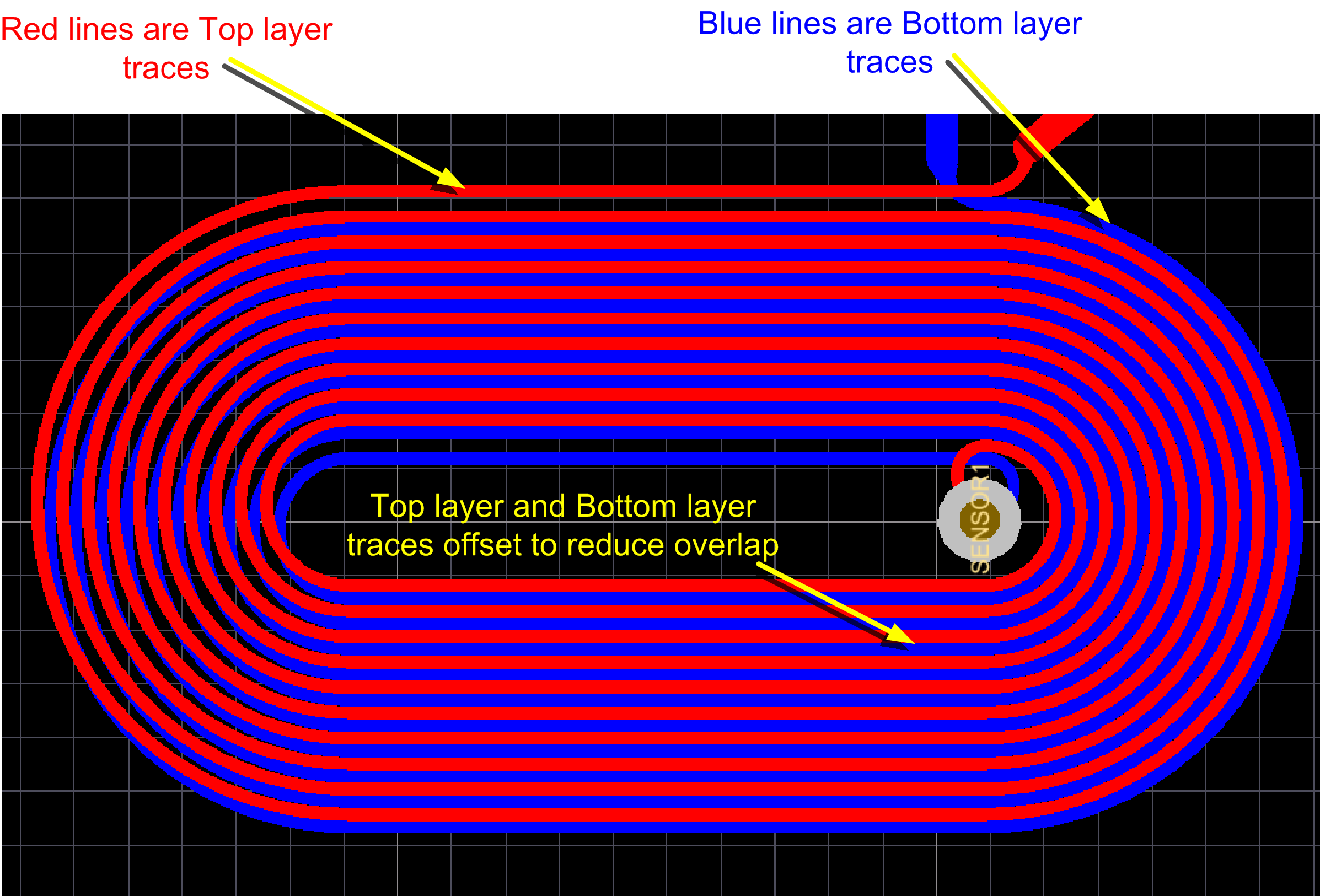
GUID-96D1CF72-A086-4BBC-BD56-4997A72080BC-low.pngFigure 2-9 Offsetting Traces to Reduce Parasitic Capacitance