SNOAA94 june 2023 LM74900-Q1 , LM74910-Q1
- 1
- Abstract
- Trademarks
- 1 LM749x0-Q1 Ideal Diode Controller Overview
- 2 Design 1: Automotive Reverse Battery Protection with Overvoltage, Undervoltage and Overcurrent Protection with Fault Output
- 3 Design 2: LM749x0-Q1 as Ideal Diode Controller with Current Monitoring, Overcurrent and Undervoltage Fault Indication
- 4 Design 3: LM749x0-Q1 as High Side Driver with Undervoltage, Overvoltage and Overcurrent Protection
- 5 Feature Comparison: LM749x0-Q1 as Ideal Diode FET and High Side Driver Topology
- 6 Design 4: Dual Supply OR-ing with Common Powerpath Disconnect Function
- 7 Design 5: LM749x0-Q1 as Priority Power MUX Controller
- 8 Feature Comparison: Dual OR-ing and Priority Power MUX Controller Topologies
- 9 Summary
- 10References
1 LM749x0-Q1 Ideal Diode Controller Overview
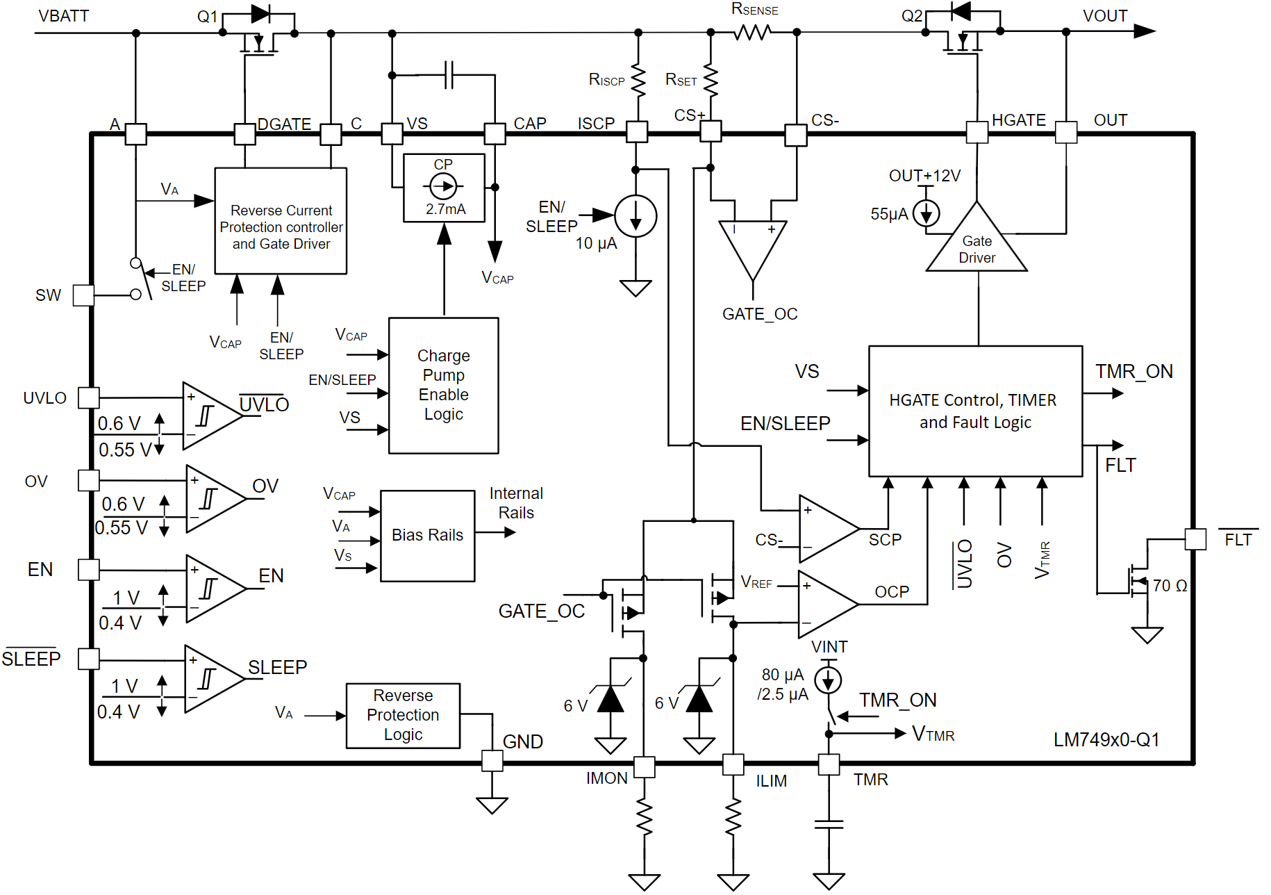
The LM749x0-Q1 family of Ideal Diode controller drive back-to-back external N-Channel MOSFETs to realize low loss power path protection with circuit breaker, under and over voltage protection functionality. The wide input supply of 3 V to 65 V allows protection and control of 12-V and 24-V automotive battery powered ECUs. The device can withstand and protect the loads from negative supply voltages down to –65 V. An integrated ideal diode controller (DGATE) drives the first MOSFET to replace a Schottky diode for reverse input protection and output voltage holdup. With a second MOSFET in the power path the device allows load disconnect (ON/OFF control) and overvoltage protection using HGATE control. The device features an adjustable overvoltage cut-off protection feature. With Common Drain configuration of the power MOSFETs, the mid-point can be used for OR-ing designs using another ideal diode. The LM749x0-Q1 has a maximum voltage rating of 65 V. The device has accurate current sensing output (IMON) with typical accuracy of (+/-10%) enabling systems for energy management. The device has integrated two level over current protection with FLT output with complete ability for adjustments of thresholds and response time. Auto-retry and latch-off fault behavior can be configured. The device offers adjustable over voltage and under voltage protection, providing robust load disconnect in case of voltage transient events.
LM749x0-Q1 features two different low power modes based on status of EN and SLEEP pin. In SLEEP mode (SLEEP =Low, EN=High) the device consumes only 6-μA current by turning off both the external MOSFET gate drives and internal charge pump but at the same time providing internal bypass path to power up always ON loads with limited current capacity. With the enable pin low, device enters into ultra low power mode by completely cutting off loads with typical current consumption of 2.87 μA. The high voltage rating of LM749x0-Q1 helps to simplify the system designs for automotive ISO7637 protection. The LM749x0-Q1 is also suitable for ORing and priority power MUX applications.
 Figure 1-1 Functional Block
Diagram