SNOAAA7 April 2024 LMG3522R030
4 Simulation Results
This section presents simulation results to verify the theory and code implementation. See Table 2-1 for the power stage parameters.
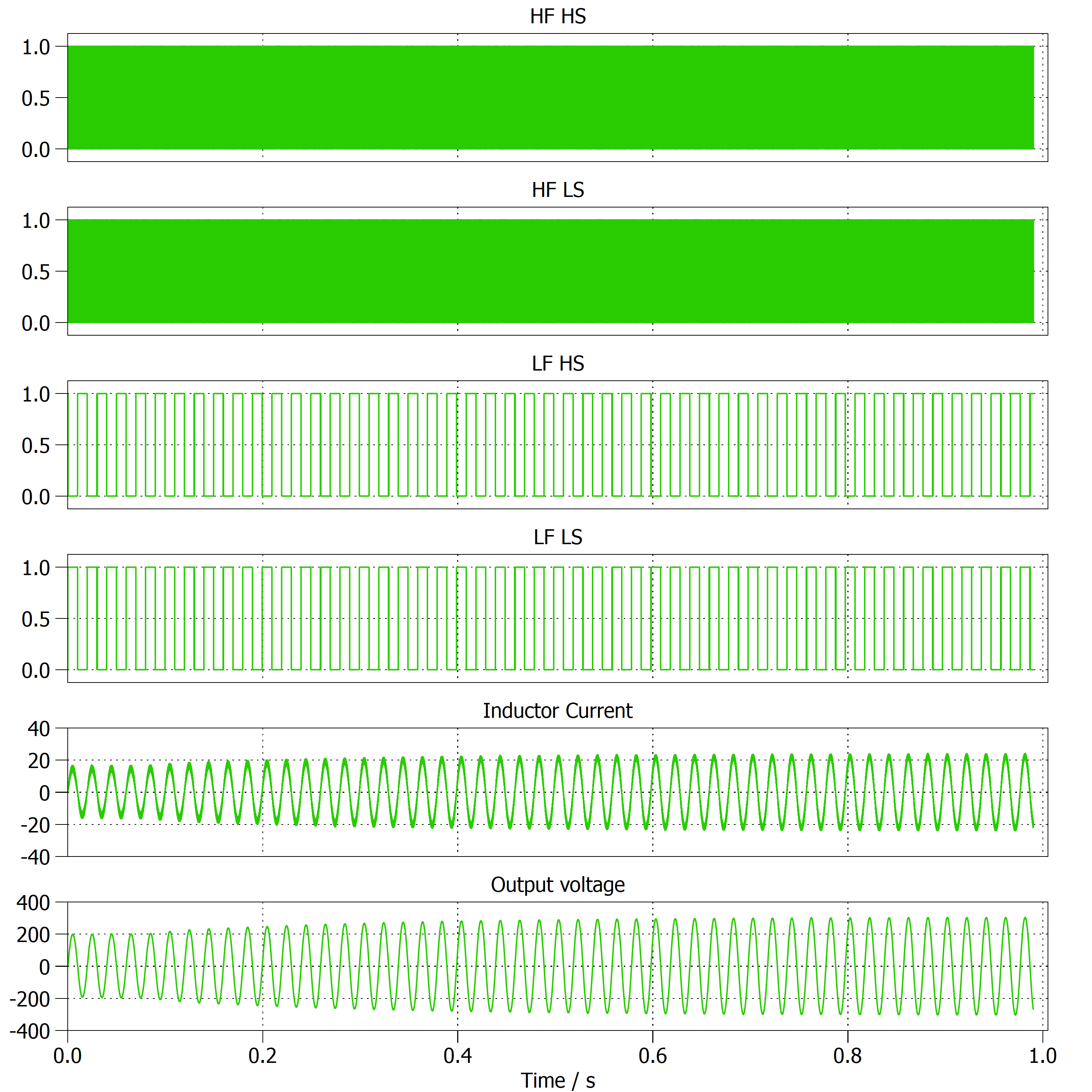
During the start-up process, to avoid a voltage surge, the initial value of the RMS array is set to 70. From start-up to 95% of the final value is defined as the settle time. Figure 4-1 shows low-frequency bridge switches at 50Hz, and high-frequency bridge switches at 100kHz. In the zero crossing, some glitches happened because of the error signal, this can be undermined by increasing the threshold.
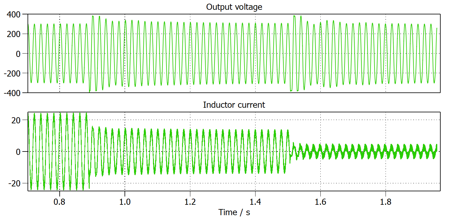
From start-up to 95% of the final value, 660ms is required. To better evaluate the performance of control parameters, a series of transient tests are set. As illustrated during the full-load and half-load situation, inductor current is a relatively standard sine wave. However, under light load, the inductor current exhibits obvious distortion. One effective way to decrease the distortion is to increase the inductance.
From Table 4-1, THD% and setting time indicate that the control system can regulate the inductor current and output voltage quickly and effectively.

 Figure 4-2 Load Transient (100% to 50% to 10%)
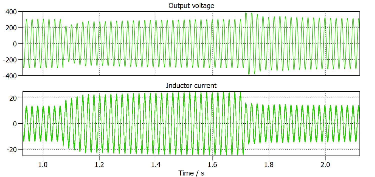
 Figure 4-3 Load Transient (50% to 100% to 50%)
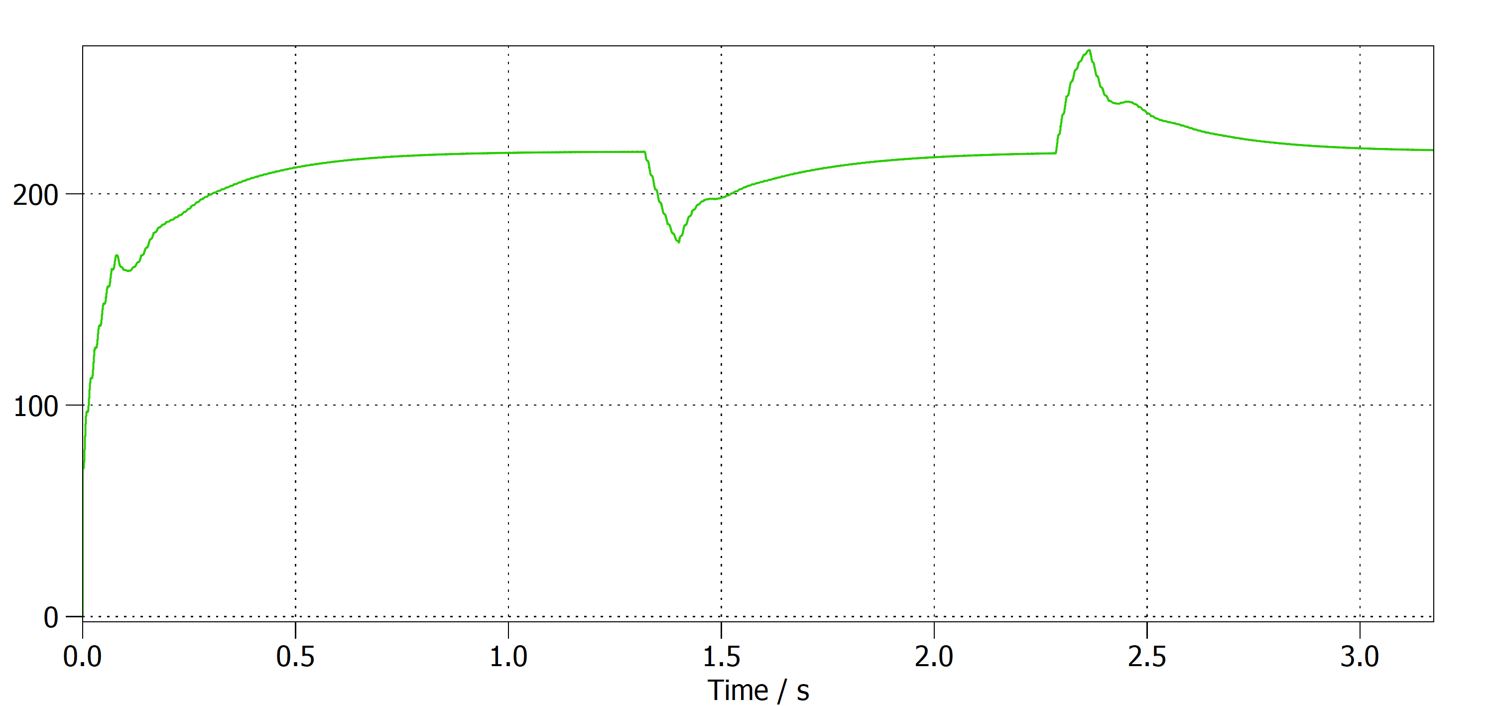
 Figure 4-4 True RMS Calculation in Load Transient
| Condition | THD% | Settle Time |
|---|---|---|
| Full load start-up | 2.7% | 0.660s |
| Full load to half-load | 2.8% | 0.281s |
| Half-load to 10%-load | 2.6% | 0.259s |
Figure 4-4 shows the output of true RMS calculation block. Note the trade-off in this block. A larger array number slows the calculation and adds additional delay to the system. This causes the output voltage to exceed the reference value because the RMS calculation lags behind the actual value. However, a short array length brings a 50Hz frequency ripple into the RMS value, which causes oscillation in the control. After many tests, a window width of 4 was found to be a good value in this model.