SNVA103B October 2005 – February 2022 LM2743
5.1 Load Transient Response
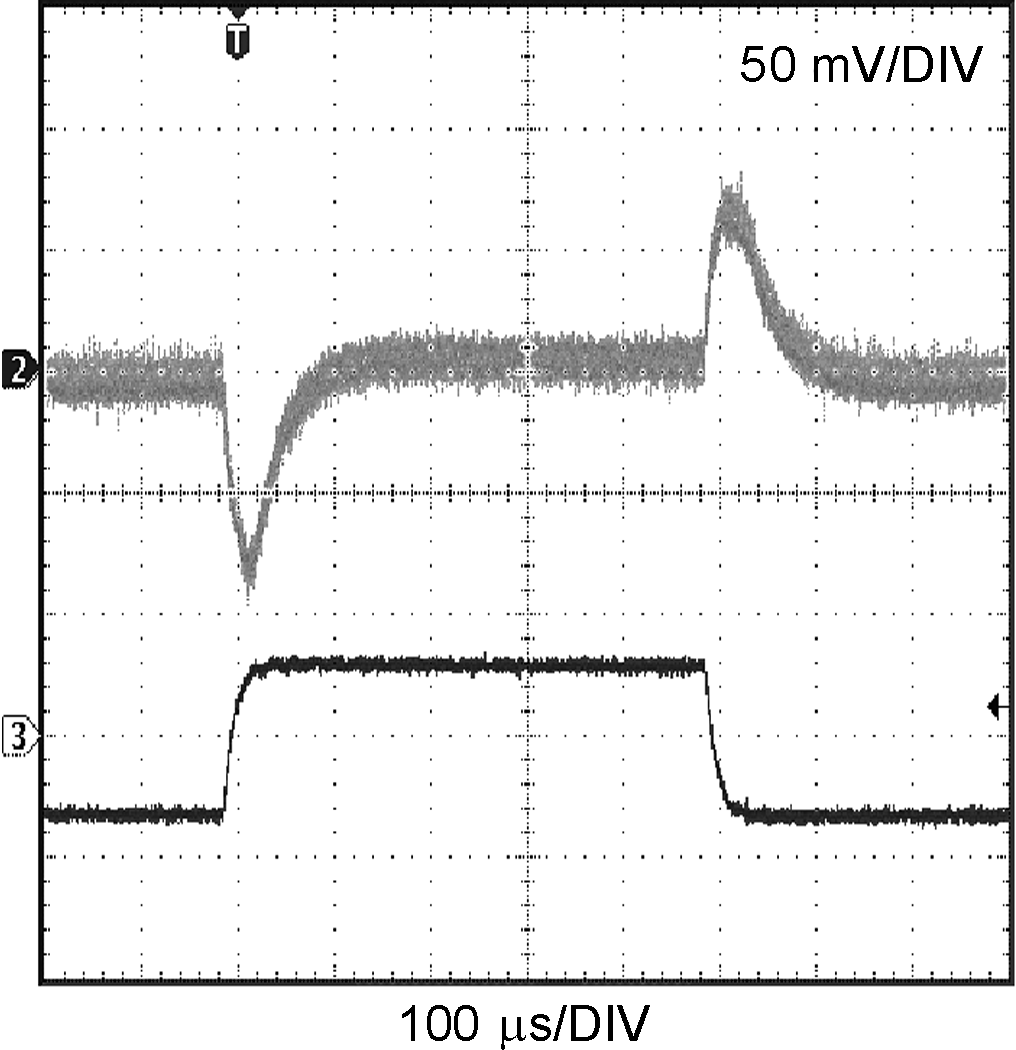
 Figure 5-1 ±3-A Load Transient Response Applied to the
Circuit in Figure 4-2 (VIN = VCC = 3.3 V and VOUT =
1.2 V). CH 2 - VOUT AC Coupled and CH 3 - 5 A/DIV
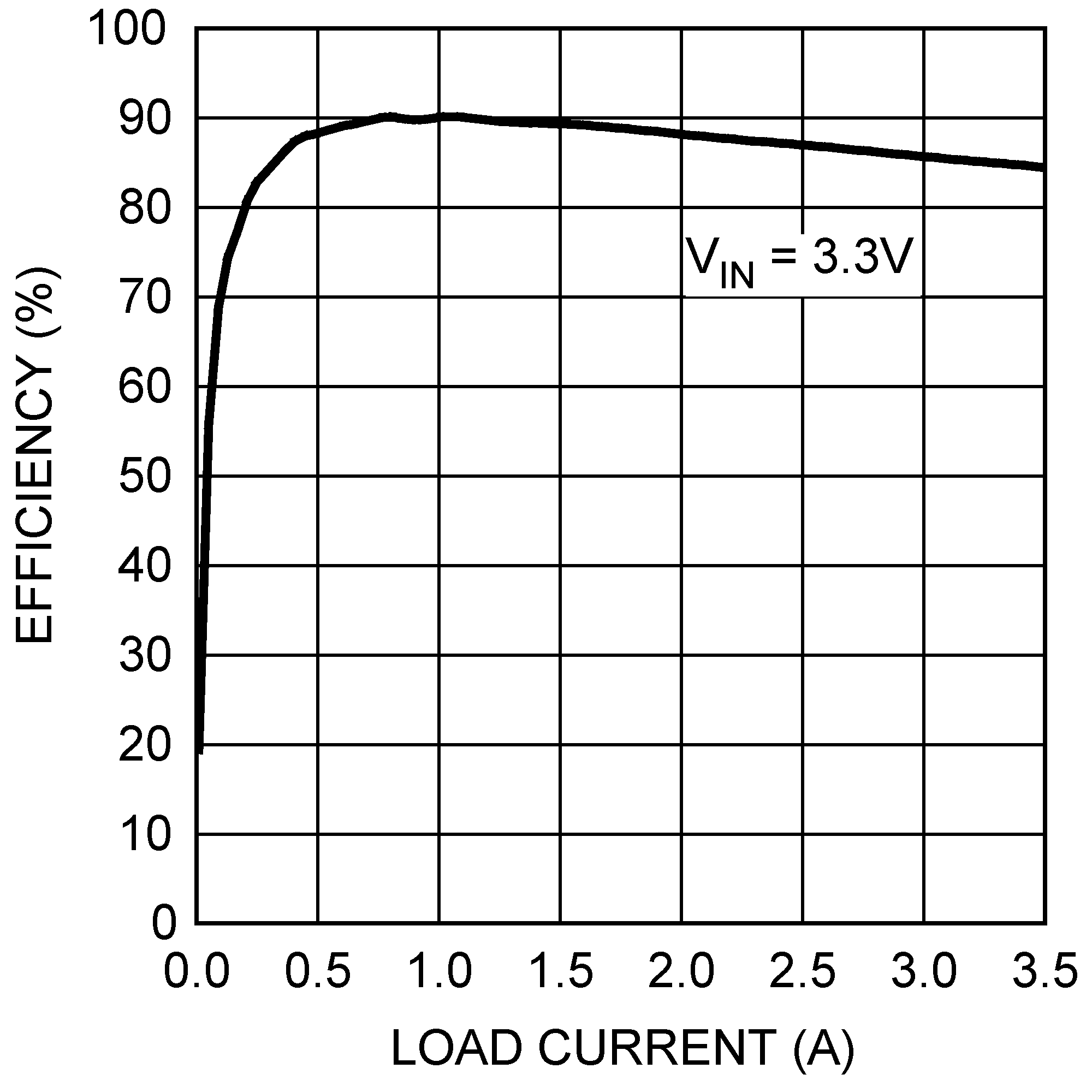
 Figure 5-2 Efficiency vs. Load Current VOUT =
1.2 V, fSW = 1 MHz