SNVA453B August 2011 – January 2022 LM10500
- Trademarks
- 1 LM10500 Overview
- 2 Adaptive Voltage Scaling Technology
- 3 Features
- 4 Applications
- 5 Evaluation Kit Overview
- 6 Typical Application Circuit
- 7 Connection Guide
- 8 Operation Guide
- 9 User’s GUI for LM10500 Evaluation Board
- 10Typical Performance Characteristics
- 11Evaluation Board Schematic
- 12Evaluation Board Bill of Materials
- 13Evaluation Board Layout
- 14Revision History
5 Evaluation Kit Overview
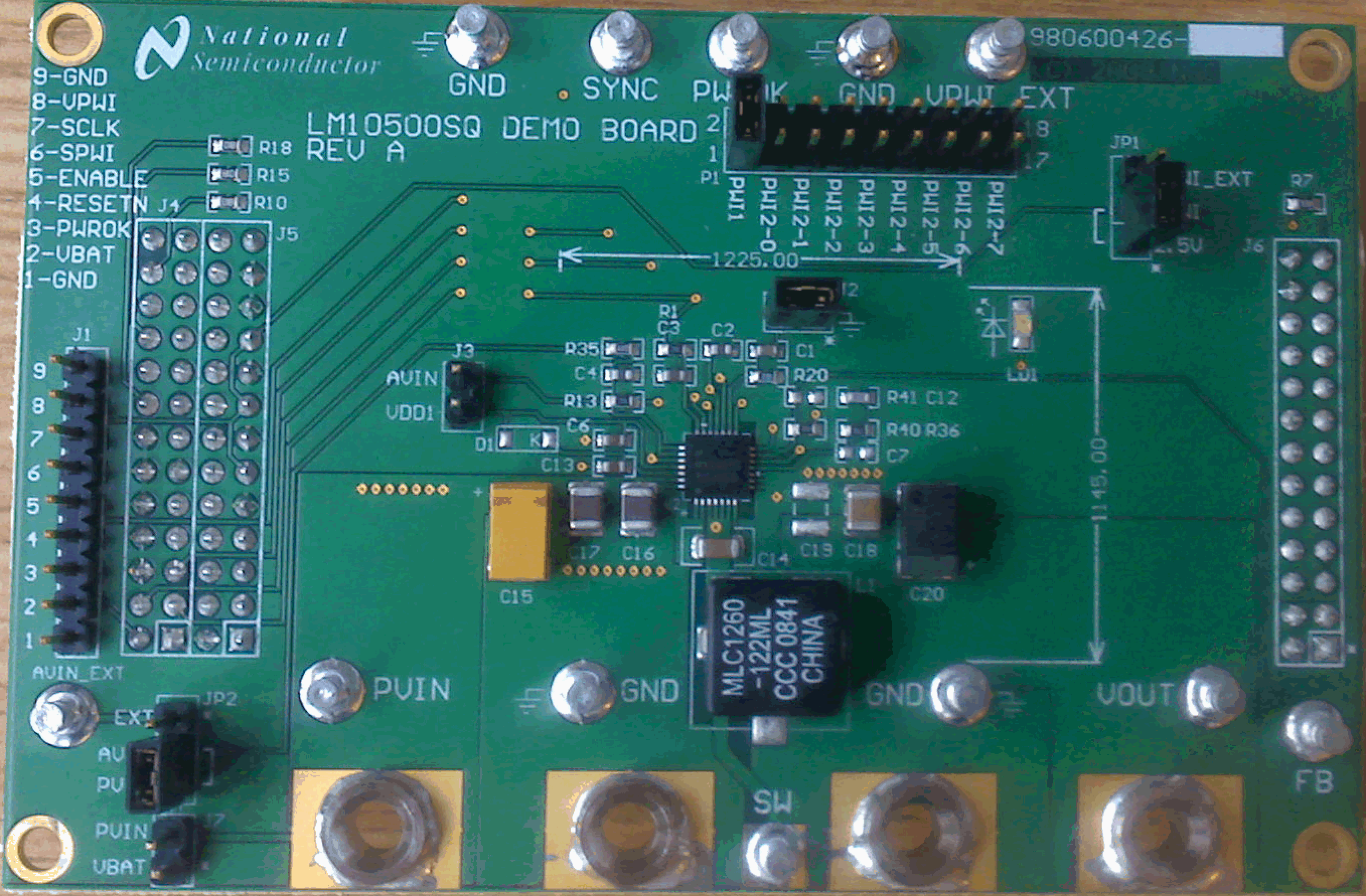
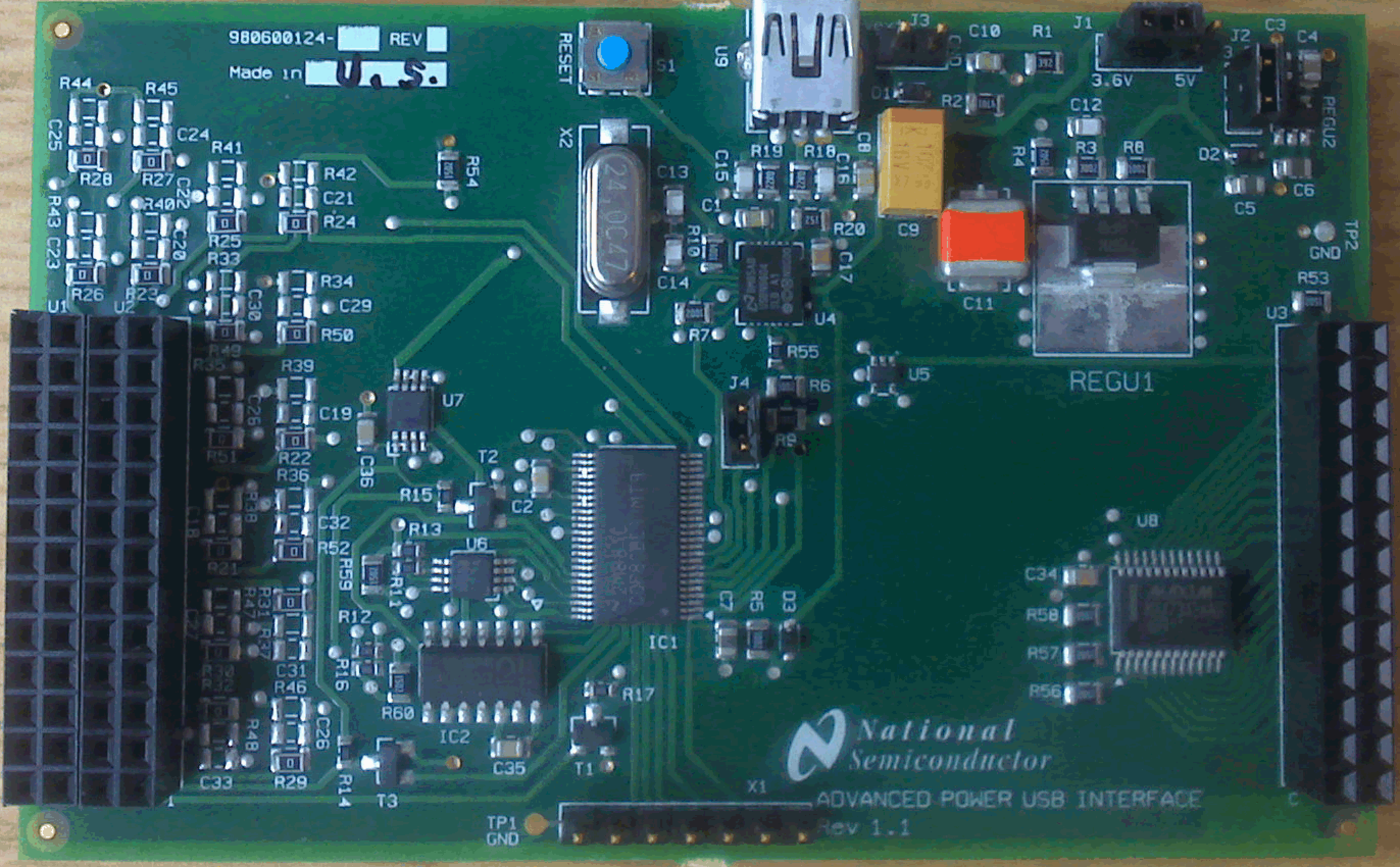
The LM10500 evaluation boards can operate standalone, communicate to a USB2PWI interface board, or to an external AVS primary. The USB2PWI interface board and a graphic user interface (GUI) are included in the evaluation kit to easily evaluate the LM10500 AVS functionality from a PC. The evaluation kit is consist of:
- LM10500 evaluation board, as shown in Figure 5-1
- USB2PWI interface board, as shown in Figure 5-2
- 5-pin mini USB cable
- A CD, including:
- LM10500 evaluation GUI
- LM10500 data sheet
- LM10500 evaluation board user's guide (this document)
There are two versions of LM10500 evaluation board: LM10500SQ-0.8EV and LM10500-1.0EV. The differences of the two versions are summarized in the following table.
| Evaluation Board ID | LM10500SQ-0.8EV | LM10500SQ-1.0EV |
| Device ID | LM10500SQ-0.8 | LM10500SQ-1.0 |
| Board Default Output Voltage, VOUT | 0.8 V | 1.2 V |
| Feedback Node Default Voltage, VFB | 0.8 V | 1.0 V |
 Figure 5-1 LM10500 Evaluation Board
 Figure 5-2 USB2PWI Interface Board