SNVA484B October   2011  – March 2024 LM5113


  1.   1
  2.   Description
  3.   IC Features
  4.   4
  5. 1Evaluation Module Overview
    1. 1.1 Introduction
    2. 1.2 Kit Contents
  6. 2Hardware
    1. 2.1 Powering and Loading Considerations
      1. 2.1.1 Proper Board Connection
      2. 2.1.2 Source Power
      3. 2.1.3 Output Current Derating
      4. 2.1.4 Air Flow
      5. 2.1.5 Quick Start-Up Procedure
  7. 3Implementation Results
    1. 3.1 Performance Characteristics
  8. 448V to 3.3V Conversion
  9. 5Hardware Design Files
    1. 5.1 Evaluation Board Schematic
    2. 5.2 PCB Layouts
    3. 5.3 Bill of Materials (BOM)
  10. 6Additional Information
    1. 6.1 Trademarks
  11. 7Revision History

Proper Board Connection

Figure 3-2 depicts the typical evaluation setup. The source power is connected to the J1 (VIN) and the J3 (GND). The load is connected to the J2 (VOUT) and the J4 (GND). Be sure to choose the correct connector and wire size. The input and output voltage must be monitored directly at the terminals of the board. The voltage drop across the connection wires causes inaccurate measurements.
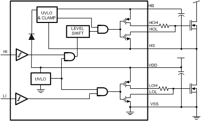
GUID-73F99523-316D-42EF-AE3E-5814EC418D95-low.gifFigure 2-1 Simplified Block Diagram of LM5113
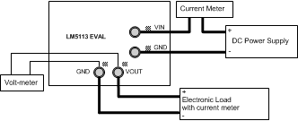
GUID-DFCEB890-CC0E-400C-8E6E-6B7C1E8101E8-low.gifFigure 2-2 Typical Evaluation Setup