SNVAA80 July 2024 LM5177 , LM51770
5 Application Measurements
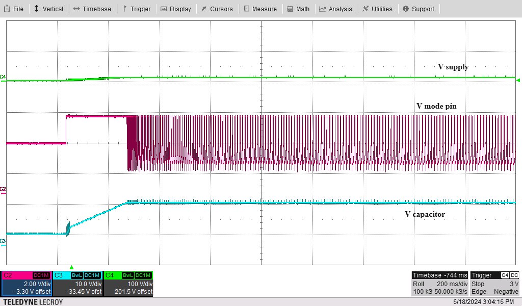
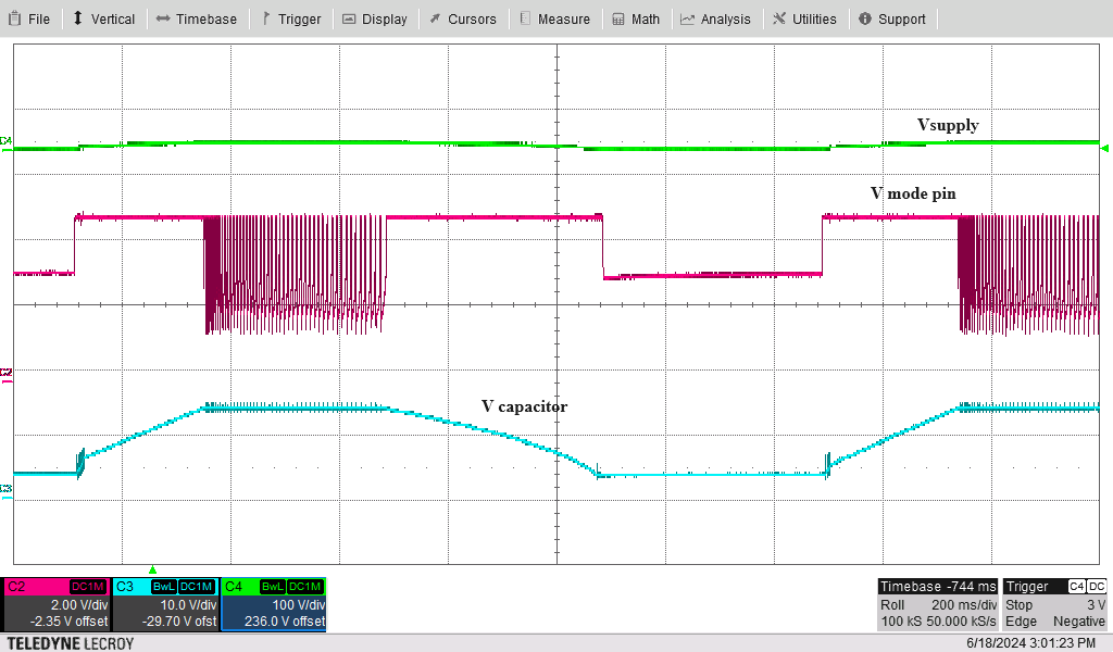
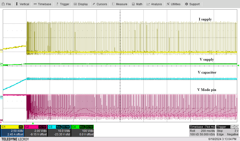
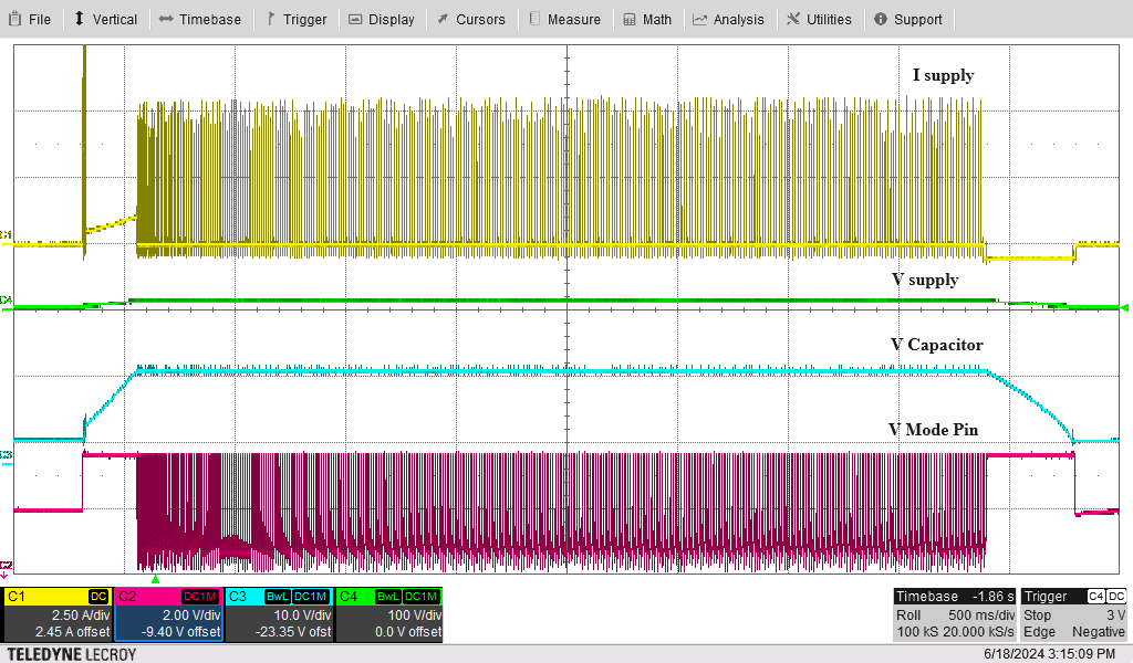
To verify that the designed controllers for the MODE pin work correctly, tests are conducted using the LM5177 Buck-Boost Controller Evaluation Module. The results, displayed in Figure 5-1 through Figure 5-4, demonstrate a smooth shift from constant current to constant voltage charging of the storage element when using the MODE pin control. However, a small hysteresis, caused by the switching delay of the MOSFET, is noticeable during the transitions between FPWM and PSM modes, leading to a minor ripple in the charging voltage. An initial bias of 5V is applied to the storage element to bypass the internal low voltage protection of the controller. When the storage voltage reaches the desired voltages, the reference voltage from the voltage divider circuit rises to 1.24V, causing the cathode voltage of the TLV431 to drop from VCC to 1.8V.
 Figure 5-1 Constant Voltage
Charging
 Figure 5-2 Constant Voltage Charging and
Discharging
 Figure 5-3 Constant Voltage Charging With
Supply Current
 Figure 5-4 Constant Voltage Charging and
Discharging With Supply Current