SNVAA87 august 2023 LMR38020
4.2 Typical Switching Waveforms Under Steady State
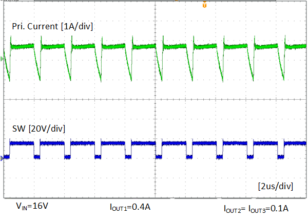
 Figure 4-5 Steady State When
VIN = 16 V, IOUT1 = 0.4 A, IOUT2 =
IOUT3 = 0.1 A
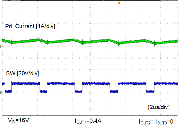
 Figure 4-7 Steady State When
VIN = 16 V, IOUT1 = 0.4 A, IOUT2 =
IOUT3 = 0 A
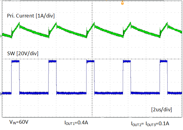
 Figure 4-6 Steady State When
VIN = 60 V, IOUT1 = 0.4 A, IOUT2 =
IOUT3 = 0.1 A
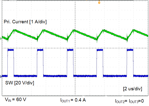
 Figure 4-8 Steady State When
VIN = 60 V, IOUT1 = 0.4 A, IOUT2 =
IOUT3 = 0 A
Figure 4-8 Steady State When
VIN = 60 V, IOUT1 = 0.4 A, IOUT2 =
IOUT3 = 0 AIn Figure 4-7, the fsw is higher than in the typical operation. This normally happens when VIN = VIN_MIN and D > 0.5, where toff is small, the primary current will hit the negative peak current limit. The LMR38020 turns off the LS and start a new cycle. In this case, the output regulation when VIN = VIN_MIN need to be checked to make sure that satisfies the system requirement. The VOUT2 = VOUT3 = 10 V under this application.