LP2998/LP2998-Q1 DDR Termination Regulator
1 Features
- AEC-Q100 Test Guidance with the following results (SO PowerPAD-8):
- Device HBM ESD Classification Level H1C
- Junction Temperature Range –40°C to 125°C
- 1.35 V Minimum VDDQ
- Source and Sink Current
- Low Output Voltage Offset
- No External Resistors Required
- Linear Topology
- Suspend to Ram (STR) Functionality
- Low External Component Count
- Thermal Shutdown
2 Applications
- DDR1, DDR2, DDR3, and DDR3L Termination Voltage
- Automotive Infotainment
- FPGA
- Industrial/Medical PC
- SSTL-18, SSTL-2, and SSTL-3 Termination
- HSTL Termination
3 Description
The LP2998 linear regulator is designed to meet JEDEC SSTL-2 and JEDEC SSTL-18 specifications for termination of DDR-SDRAM and DDR2 memory. The device also supports DDR3 and DDR3L VTT bus termination with VDDQ min of 1.35 V. The device contains a high-speed operational amplifier to provide excellent response to load transients. The output stage prevents shoot through while delivering 1.5 A continuous current and transient peaks up to 3 A in the application as required for DDR-SDRAM termination. The LP2998 also incorporates a VSENSE pin to provide superior load regulation and a VREF output as a reference for the chipset and DIMMs.
An additional feature found on the LP2998 is an active low shutdown (SD) pin that provides Suspend To RAM (STR) functionality. When SD is pulled low the VTT output will tri-state providing a high impedance output, but, VREF will remain active. A power savings advantage can be obtained in this mode through lower quiescent current.
Device Information(1)
| PART NUMBER | PACKAGE | BODY SIZE (NOM) |
|---|---|---|
| LP2998 | SO PowerPAD™ (8) | 4.89 mm x 3.90 mm |
| LP2998 | SOIC (8) | 4.90 mm x 3.91 mm |
| LP2998-Q1 | SO PowerPAD™ (8) | 4.89 mm x 3.90 mm |
- For all available packages, see the orderable addendum at the end of the datasheet.
4 Simplified Schematic

5 Revision History
Changes from J Revision (December 2013) to K Revision
- Added DDR3 support throughout datasheetGo
- Changed formatting to match new TI datasheet guidelines; added Device Information and Handling Ratings tables, Power Supply, Layout Examples, and Device and Documentation Support sections; reformatted Detailed Description and Application and Implementation sections. Go
- Changed Electrical Char table condition statement Go
Changes from I Revision (April 2013) to J Revision
6 Pin Configuration and Functions
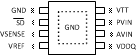
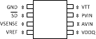
Pin Functions
| PIN | ||
|---|---|---|
| NUMBER | TYPE | DESCRIPTION |
| 1 | GND | Ground |
| 2 | SD | Shutdown |
| 3 | VSENSE | Feedback pin for regulating VTT. |
| 4 | VREF | Buffered internal reference voltage of VDDQ/2 |
| 5 | VDDQ | Input for internal reference equal to VDDQ/2 |
| 6 | AVIN | Analog input pin |
| 7 | PVIN | Power input pin |
| 8 | VTT | Output voltage for connection to termination resistors |
| EP | Exposed pad thermal connection. Connect to Ground. | |
6.1 Pin Descriptions
| AVIN AND PVIN | AVIN and PVIN are the input supply pins for the LP2998. AVIN is used to supply all the internal control circuitry. PVIN, however, is used exclusively to provide the rail voltage for the output stage used to create VTT. These pins have the capability to work off separate supplies depending on the application. Higher voltages on PVIN will increase the maximum continuous output current because of output RDSON limitations at voltages close to VTT. The disadvantage of high values of PVIN is that the internal power loss will also increase, thermally limiting the design. For SSTL-2 applications, a good compromise would be to connect the AVIN and PVIN directly together at 2.5 V. This eliminates the need for bypassing the two supply pins separately. The only limitation on input voltage selection is that PVIN must be equal to or lower than AVIN. It is recommended to connect PVIN to voltage rails equal to or less than 3.3 V to prevent the thermal limit from tripping because of excessive internal power dissipation. If the junction temperature exceeds the thermal shutdown than the part will enter a shutdown state identical to the manual shutdown where VTT is tri-stated and VREF remains active. |
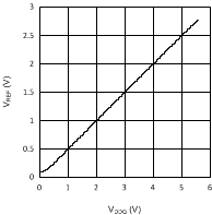
| VDDQ | VDDQ is the input used to create the internal reference voltage for regulating VTT. The reference voltage is generated from a resistor divider of two internal 50 kΩ resistors. This ensures that VTT will track VDDQ / 2 precisely. The optimal implementation of VDDQ is as a remote sense. This can be achieved by connecting VDDQ directly to the 2.5 V rail at the DIMM instead of AVIN and PVIN. This ensures that the reference voltage tracks the DDR memory rails precisely without a large voltage drop from the power lines. For SSTL-2 applications VDDQ will be a 2.5 V signal, which will create a 1.25 V termination voltage at VTT (See Electrical Characteristics Table for exact values of VTT over temperature). |
|
VSENSE |
The purpose of the sense pin is to provide improved remote load regulation. In most motherboard applications the termination resistors will connect to VTT in a long plane. If the output voltage was regulated only at the output of the LP2998 then the long trace will cause a significant IR drop resulting in a termination voltage lower at one end of the bus than the other. The VSENSE pin can be used to improve this performance, by connecting it to the middle of the bus. This will provide a better distribution across the entire termination bus. If remote load regulation is not used then the VSENSE pin must still be connected to VTT. Care should be taken when a long VSENSE trace is implemented in close proximity to the memory. Noise pickup in the VSENSE trace can cause problems with precise regulation of VTT. A small 0.1 uF ceramic capacitor placed next to the VSENSE pin can help filter any high frequency signals and preventing errors. |
| SHUTDOWN | The LP2998 contains an active low shutdown pin that can be used to tri-state VTT. During shutdown VTT should not be exposed to voltages that exceed AVIN. With the shutdown pin asserted low the quiescent current of the LP2998 will drop, however, VDDQ will always maintain its constant impedance of 100 kΩ for generating the internal reference. Therefore, to calculate the total power loss in shutdown both currents need to be considered. For more information refer to the Thermal Dissipation section. The shutdown pin also has an internal pull-up current, therefore to turn the part on the shutdown pin can either be connected to AVIN or left open. |
| VREF | VREF provides the buffered output of the internal reference voltage VDDQ / 2. This output should be used to provide the reference voltage for the Northbridge chipset and memory. Since these inputs are typically an extremely high impedance, there should be little current drawn from VREF. For improved performance, an output bypass capacitor can be used, located close to the pin, to help with noise. A ceramic capacitor in the range of 0.1 µF to 0.01 µF is recommended. This output remains active during the shutdown state and thermal shutdown events for the suspend to RAM functionality. |
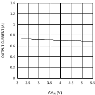
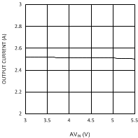
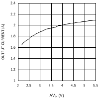
| VTT | VTT is the regulated output that is used to terminate the bus resistors. It is capable of sinking and sourcing current while regulating the output precisely to VDDQ / 2. The LP2998 is designed to handle peak transient currents of up to ± 3 A with a fast transient response. The maximum continuous current is a function of VIN and can be viewed in the Typical Characteristics section. If a transient is expected to last above the maximum continuous current rating for a significant amount of time then the output capacitor should be sized large enough to prevent an excessive voltage drop. Despite the fact that the LP2998 is designed to handle large transient output currents it is not capable of handling these for long durations, under all conditions. The reason for this is the standard packages are not able to thermally dissipate the heat as a result of the internal power loss. If large currents are required for longer durations, then care should be taken to ensure that the maximum junction temperature is not exceeded. Proper thermal derating should always be used (please refer to the Thermal Dissipation section). If the junction temperature exceeds the thermal shutdown point than VTT will tri-state until the part returns below the hysteretic trip-point. |
7 Specifications
7.1 Absolute Maximum Ratings (1)(2)
over operating free-air temperature range (unless otherwise noted)| MIN | MAX | UNIT | |
|---|---|---|---|
| AVIN to GND | −0.3 | 6 | V |
| PVIN to GND | –0.3 | AVIN | V |
| VDDQ(3) | −0.3 | 6 | V |
| Junction temperature | 150 | °C | |
| Lead temperature (soldering, 10 sec) | 260 | °C |
7.2 Handling Ratings: LP2998
| MIN | MAX | UNIT | |||
|---|---|---|---|---|---|
| Tstg | Storage temperature range | −65 | 150 | °C | |
| V(ESD) | Electrostatic discharge | Human body model (HBM), per ANSI/ESDA/JEDEC JS-001, all pins(1) | −1000 | 1000 | V |
7.3 Handling Ratings: LP2998-Q1
| MIN | MAX | UNIT | ||||
|---|---|---|---|---|---|---|
| Tstg | Storage temperature range | −65 | 150 | °C | ||
| V(ESD) | Electrostatic discharge | Human body model (HBM), per AEC Q100-002(1) | −1000 | 1000 | V | |
7.4 Recommended Operating Conditions
over operating free-air temperature range (unless otherwise noted)| MIN | NOM | MAX | UNIT | ||
|---|---|---|---|---|---|
| Junction temperature(1) | –40 | 125 | °C | ||
| AVIN to GND | 2.2 | 5.5 | V | ||
| PVIN supply voltage | 0 | AVIN | V | ||
| SD input voltage | 0 | AVIN | V | ||
7.5 Thermal Information
| THERMAL METRIC(1) | LP2998/LP2998-Q1 | LP2998 | UNIT | |
|---|---|---|---|---|
| SO PowerPAD | SOIC | |||
| 8 PINS | 8 PINS | |||
| RθJA | Junction-to-ambient thermal resistance | 43 | 151 | °C/W |
7.6 Electrical Characteristics
Typical limits tested at TJ = 25°C. Minimum and maximum limits apply over the full operating junction temperature range (TJ = –40°C to 125°C).(2) Unless otherwise specified, AVIN = PVIN = 2.5 V, VDDQ = 2.5 V.(3)| PARAMETER | TEST CONDITIONS | MIN | TYP | MAX | UNIT | |
|---|---|---|---|---|---|---|
| VREF | VREF voltage (DDR I) | VIN = VDDQ = 2.3 V | 1.135 | 1.158 | 1.185 | V |
| VIN = VDDQ = 2.5 V | 1.235 | 1.258 | 1.285 | |||
| VIN = VDDQ = 2.7 V | 1.335 | 1.358 | 1.385 | |||
| VREF voltage (DDR II) | PVIN = VDDQ = 1.7 V | 0.837 | 0.860 | 0.887 | ||
| PVIN = VDDQ = 1.8 V | 0.887 | 0.910 | 0.937 | |||
| PVIN = VDDQ = 1.9 V | 0.936 | 0.959 | 0.986 | |||
| VREF Voltage (DDR III) | PVIN = VDDQ = 1.35V | 0.669 | 0.684 | 0.699 | ||
| PVIN = VDDQ = 1.5V | 0.743 | 0.758 | 0.773 | |||
| PVIN = VDDQ = 1.6V | 0.793 | 0.808 | 0.823 | |||
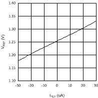
| ZVREF | VREF Output Impedance | IREF = –30 to 30 µA | 2.5 | kΩ | ||
| VTT | VTT Output Voltage (DDR I) (6) | IOUT = 0 A | V | |||
| VIN = VDDQ = 2.3 V | 1.120 | 1.159 | 1.190 | |||
| VIN = VDDQ = 2.5 V | 1.210 | 1.259 | 1.290 | |||
| VIN = VDDQ = 2.7 V | 1.320 | 1.359 | 1.390 | |||
| IOUT = ±1.5 A | ||||||
| VIN = VDDQ = 2.3 V | 1.125 | 1.159 | 1.190 | |||
| VIN = VDDQ = 2.5 V | 1.225 | 1.259 | 1.290 | |||
| VIN = VDDQ = 2.7 V | 1.325 | 1.359 | 1.390 | |||
| VTT Output Voltage (DDR II) (6) | IOUT = 0 A, AVIN = 2.5 V | V | ||||
| PVIN = VDDQ = 1.7 V | 0.822 | 0.856 | 0.887 | |||
| PVIN = VDDQ = 1.8 V | 0.874 | 0.908 | 0.939 | |||
| PVIN = VDDQ = 1.9 V | 0.923 | 0.957 | 0.988 | |||
| IOUT = ±0.5A, AVIN = 2.5 V | ||||||
| PVIN = VDDQ = 1.7 V | 0.820 | 0.856 | 0.890 | |||
| PVIN = VDDQ = 1.8 V | 0.870 | 0.908 | 0.940 | |||
| PVIN = VDDQ = 1.9 V | 0.920 | 0.957 | 0.990 | |||
| VTT Output Voltage (DDR III) (6) | IOUT = 0A, AVIN = 2.5 V | V | ||||
| PVIN = VDDQ = 1.35V | 0.656 | 0.677 | 0.698 | |||
| PVIN = VDDQ = 1.5 V | 0.731 | 0.752 | 0.773 | |||
| PVIN = VDDQ = 1.6 V | 0.781 | 0.802 | 0.823 | |||
| IOUT = 0.2 A, AVIN = 2.5V PVIN = VDDQ = 1.35V |
0.667 | 0.688 | 0.710 | |||
| IOUT = -0.2A, AVIN = 2.5V PVIN = VDDQ = 1.35V |
0.641 | 0.673 | 0.694 | |||
| IOUT = 0.4 A, AVIN = 2.5 V PVIN = VDDQ = 1.5 V |
0.740 | 0.763 | 0.786 | |||
| IOUT = –0.4 A, AVIN = 2.5 V PVIN = VDDQ = 1.5 V |
0.731 | 0.752 | 0.773 | |||
| IOUT = 0.5 A, AVIN = 2.5 V PVIN = VDDQ = 1.6 V |
0.790 | 0.813 | 0.836 | |||
| IOUT = –0.5 A, AVIN = 2.5 V PVIN = VDDQ = 1.6 V |
0.781 | 0.802 | 0.823 | |||
| VOSVtt | VTT Output Voltage Offset (VREF – VTT) for DDR I (6) | IOUT = 0 A | –30 | 0 | 30 | mV |
| IOUT = –1.5 A | –30 | 0 | 30 | |||
| IOUT = 1.5 A | –30 | 0 | 30 | |||
| VTT Output Voltage Offset (VREF – VTT) for DDR II (6) | IOUT = 0 A | –30 | 0 | 30 | ||
| IOUT = –0.5 A | –30 | 0 | 30 | |||
| IOUT = 0.5 A | –30 | 0 | 30 | |||
| VTT Output Voltage Offset (VREF – VTT) for DDR III (6) | IOUT = 0 A | –30 | 0 | 30 | ||
| IOUT = ±0.2 A | –30 | 0 | 30 | |||
| IOUT = ±0.4 A | –30 | 0 | 30 | |||
| IOUT = ±0.5 A | –30 | 0 | 30 | |||
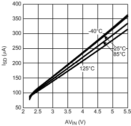
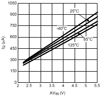
| IQ | Quiescent Current (4) | IOUT = 0 A | 320 | 500 | µA | |
| ZVDDQ | VDDQ Input Impedance | 100 | kΩ | |||
| ISD | Quiescent current in shutdown (4) | SD = 0 V | 115 | 150 | µA | |
| IQ_SD | Shutdown leakage current | SD = 0 V | 2 | 5 | ||
| VIH | Minimum Shutdown High Level | 1.9 | V | |||
| VIL | Maximum Shutdown Low Level | 0.8 | ||||
| Iv | VTT leakage current in shutdown | SD = 0 V VTT = 1.25 V |
1 | 10 | µA | |
| ISENSE | VSENSE Input current | 13 | nA | |||
| TSD | Thermal Shutdown (5) | 165 | °C | |||
| TSD_HYS | Thermal Shutdown Hysteresis | 10 | ||||
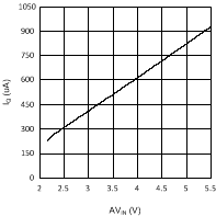
7.7 Typical Characteristics
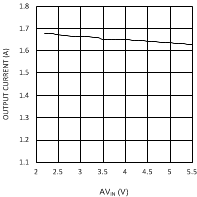
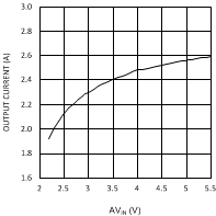
Unless otherwise specified AVIN = PVIN = 2.5 V.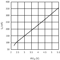
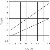
| VDDQ = 2.5 V | PVIN = 1.8 V | |
| VDDQ = 2.5 V | PVIN = 3.3 V | |
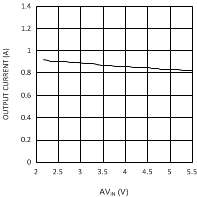
| VDDQ = 1.8 V | PVIN = 1.8 V | |
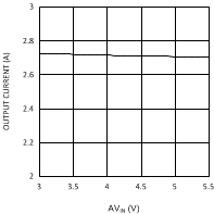
| VDDQ = 1.8 V | PVIN = 3.3 V | |||
8 Detailed Description
8.1 Overview
The LP2998 linear regulator is designed to meet JEDEC SSTL-2 and JEDEC SSTL-18 specifications for termination of DDR-SDRAM and DDR2 memory. The device also supports DDR3 and DDR3L VTT bus termination with VDDQ min of 1.35 V. The device contains a high-speed operational amplifier to provide excellent response to load transients. The output stage prevents shoot through while delivering 1.5 A continuous current and transient peaks up to 3 A in the application as required for DDR-SDRAM termination.
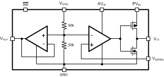
8.2 Functional Block Diagram
8.3 Feature Description
The LP2998 is a linear bus termination regulator designed to meet the JEDEC requirements of SSTL-2 and SSTL-18. The output, VTT is capable of sinking and sourcing current while regulating the output voltage equal to VDDQ / 2. The output stage has been designed to maintain excellent load regulation while preventing shoot through. The LP2998 also incorporates two distinct power rails that separates the analog circuitry from the power output stage. This allows a split rail approach to be utilized to decrease internal power dissipation. It also permits the LP2998 to provide a termination solution for DDR3-SDRAM and DDR3L-SDRAM memory.
8.4 Device Functional Modes
The LP2998 can also be used to provide a termination voltage for other logic schemes such as SSTL-3 or HSTL. Series Stub Termination Logic (SSTL) was created to improve signal integrity of the data transmission across the memory bus. This termination scheme is essential to prevent data error from signal reflections while transmitting at high frequencies encountered with DDR-SDRAM. The most common form of termination is Class II single parallel termination. This involves one RS series resistor from the chipset to the memory and one RT termination resistor. Typical values for RS and RT are 25 Ω, although these can be changed to scale the current requirements from the LP2998. This implementation can be seen below in Figure 16.
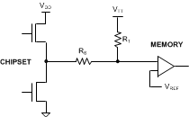 Figure 16. SSTL-Termination Scheme