SNVSA56B May   2015  – February 2017 LM2776

PRODUCTION DATA.  

  1. Features
  2. Applications
  3. Description
    1.     Device Images
      1.      Typical Application
      2.      Output Impedance vs Input Voltage IOUT = 100 mA
  4. Revision History
  5. Pin Configuration and Functions
    1.     Pin Functions
  6. Specifications
    1. 6.1 Absolute Maximum Ratings
    2. 6.2 ESD Ratings
    3. 6.3 Recommended Operating Conditions
    4. 6.4 Thermal Information
    5. 6.5 Electrical Characteristics
    6. 6.6 Switching Characteristics
    7. 6.7 Typical Characteristics
  7. Detailed Description
    1. 7.1 Overview
    2. 7.2 Functional Block Diagram
    3. 7.3 Feature Description
      1. 7.3.1 Input Current Limit
      2. 7.3.2 PFM Operation
      3. 7.3.3 Output Discharge
      4. 7.3.4 Thermal Shutdown
      5. 7.3.5 Undervoltage Lockout
    4. 7.4 Device Functional Modes
      1. 7.4.1 Shutdown Mode
      2. 7.4.2 Enable Mode
  8. Application and Implementation
    1. 8.1 Application Information
    2. 8.2 Typical Application - Voltage Inverter
      1. 8.2.1 Design Requirements
      2. 8.2.2 Detailed Design Requirements
        1. 8.2.2.1 Efficiency
        2. 8.2.2.2 Power Dissipation
        3. 8.2.2.3 Capacitor Selection
        4. 8.2.2.4 Output Capacitor and Output Voltage Ripple
        5. 8.2.2.5 Input Capacitor
        6. 8.2.2.6 Flying Capacitor
      3. 8.2.3 Application Curve
  9. Power Supply Recommendations
  10. 10Layout
    1. 10.1 Layout Guidelines
    2. 10.2 Layout Example
  11. 11Device and Documentation Support
    1. 11.1 Device Support
      1. 11.1.1 Third-Party Products Disclaimer
    2. 11.2 Receiving Notification of Documentation Updates
    3. 11.3 Community Resources
    4. 11.4 Trademarks
    5. 11.5 Electrostatic Discharge Caution
    6. 11.6 Glossary
  12. 12Mechanical, Packaging, and Orderable Information

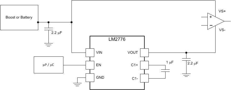
Typical Application - Voltage Inverter

LM2776 system.gifFigure 18. Voltage Inverter