SNVU191B October 2012 – December 2021 LMR12020
6 Performance Characteristics
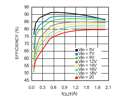
 Figure 6-1 Efficiency vs. Load Current LMR12020
VOUT = 5 V
 Figure 6-3 Load Transient Waveforms
LMR12020, VOUT = 5 V, VIN = 12 V, IOUT =
200 mA to 2 A
 Figure 6-5 Start-Up Waveform,
VOUT = 3.3 V
 Figure 6-7 Switching Node and Output
Voltage Waveforms VIN = 12 V, IOUT = 2 A
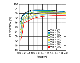
 Figure 6-2 Efficiency vs. Load Current LMR12020
VOUT = 3.3 V
 Figure 6-4 Load Transient Waveforms
LMR12020, VOUT = 3.3 V, VIN = 12 V, IOUT =
200 mA to 2 A
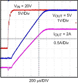
 Figure 6-6 Start-Up Waveform,
VOUT = 5 V