SPRACM3E August 2021 – January 2023 F29H850TU , F29H859TU-Q1 , TMS320F280021 , TMS320F280021-Q1 , TMS320F280023 , TMS320F280023-Q1 , TMS320F280023C , TMS320F280025 , TMS320F280025-Q1 , TMS320F280025C , TMS320F280025C-Q1 , TMS320F280033 , TMS320F280034 , TMS320F280034-Q1 , TMS320F280036-Q1 , TMS320F280036C-Q1 , TMS320F280037 , TMS320F280037-Q1 , TMS320F280037C , TMS320F280037C-Q1 , TMS320F280038-Q1 , TMS320F280038C-Q1 , TMS320F280039 , TMS320F280039-Q1 , TMS320F280039C , TMS320F280039C-Q1 , TMS320F280040-Q1 , TMS320F280040C-Q1 , TMS320F280041 , TMS320F280041-Q1 , TMS320F280041C , TMS320F280041C-Q1 , TMS320F280045 , TMS320F280048-Q1 , TMS320F280048C-Q1 , TMS320F280049 , TMS320F280049-Q1 , TMS320F280049C , TMS320F280049C-Q1 , TMS320F28384D , TMS320F28384S , TMS320F28386D , TMS320F28386S , TMS320F28388D , TMS320F28388S , TMS320F28P650DH , TMS320F28P650DK , TMS320F28P650SH , TMS320F28P650SK , TMS320F28P659DH-Q1 , TMS320F28P659DK-Q1 , TMS320F28P659SH-Q1
- Using the Fast Serial Interface (FSI) With Multiple Devices in an Application
- Trademarks
- 1Introduction to the FSI Module
- 2FSI Applications
- 3Handshake Mechanism
- 4Sending and Receiving FSI Data Frames
- 5Daisy-Chain Topology Tests
- 6Star Topology Tests
-
7Event Synchronization Over FSI
- 7.1 Introduction
- 7.2 C2000Ware FSI EPWM Sync Examples
- 7.3 Additional Tips and Usage of FSI Event Sync
- 8References
- 9Revision History
5.2.2 Hardware Control
- Test condition
Device 1 sends data -> Device 2 while receiving the data also passes it to Device 3 -> Device 3 while receiving the data also passes it to Device 1 -> Device 1 receives data and verifies it matches the originally sent Tx data.
- Test case
Data length of 8 words, 1 data lines, TXCLK= 30 MHz, with Setting ④ (Table 5-1) enabled.
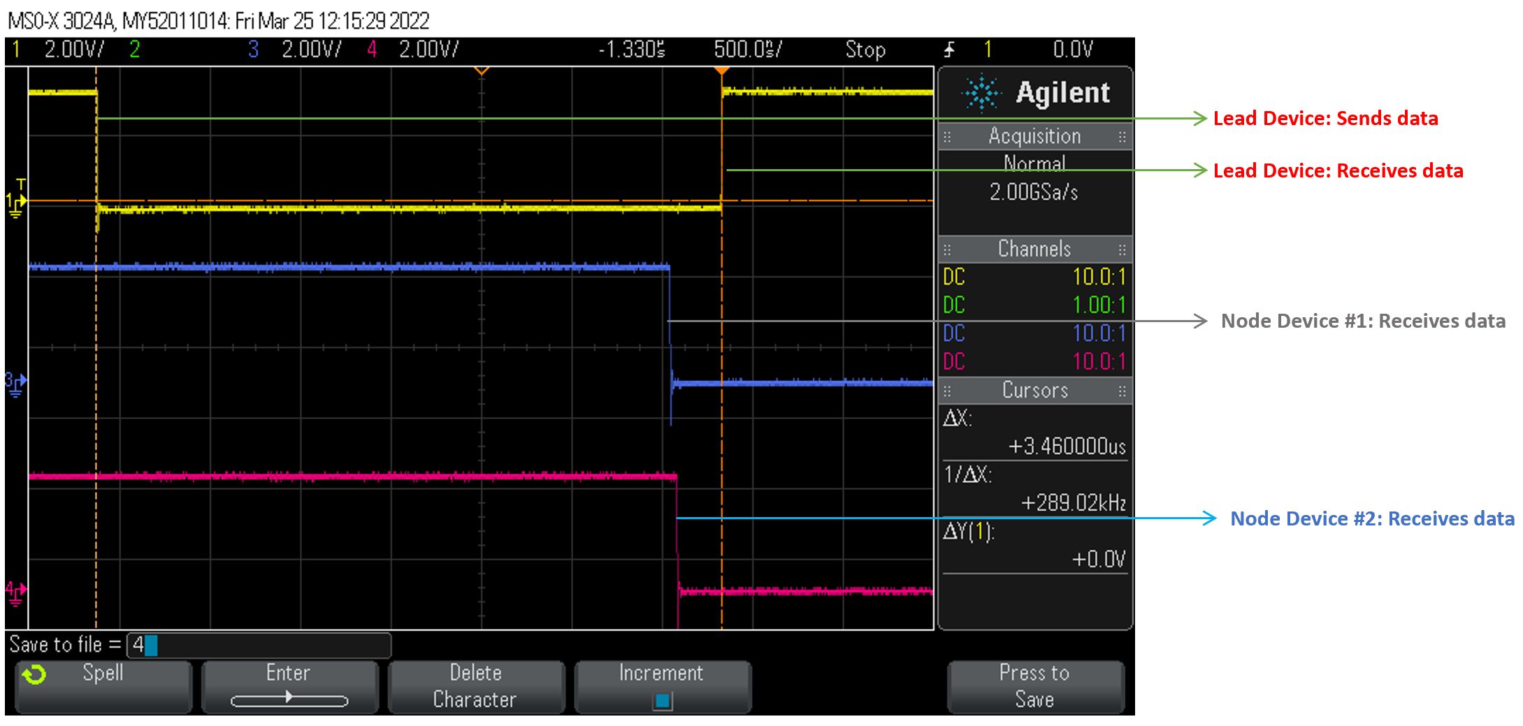
In the tests, GPIOs are toggled within software when specific events occur during the communication and measured using an oscilloscope to obtain the respective timing data. In the figures below, the yellow signal represents the GPIO toggling of Device 1 (Lead device), the blue signal represents the GPIO toggling of Device 2 (Node device), and the magenta signal represents the GPIO toggling of Device 3 (Node device).
 Figure 5-11 FSI Communication With
Hardware Control Among Three Devices
Figure 5-11 FSI Communication With
Hardware Control Among Three DevicesFor this case, the time needed for the data transmission to complete the three device daisy-chain loop is 3.46µs, as shown in Figure 5-11. As can be seen in the figure, the Device 2 and Device 3 receive the data almost simultaneously. Also note that, Device 1 receives the data packet even before it completes servicing the TX frame interrupt generated after packet transmission and because of this the GPIO toggling is delayed even though the packet is received much earlier.
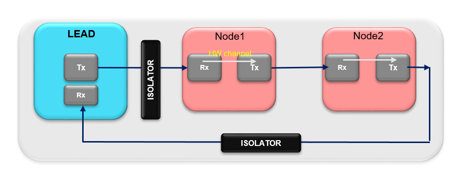
 Figure 5-12 Three Node Setup Used to
Generate the Results for Hardware Control
Figure 5-12 Three Node Setup Used to
Generate the Results for Hardware ControlNote that these results are generated by assuming the Device 2 and Device 3 are not isolated from each other. Isolators are kept only for Device 1. The setup used is shown in Figure 5-12. This is because the signal distortion effects get accumulated with each isolator and this leads to communication errors.
- Because the HW control uses a pass-through connection in the hardware, effectively all the devices in the network are wired together. This makes it impossible to perform any conditioning on the signal in the hardware.
- The signal distortion effects of isolators and other circuitry on FSI clock and data lines are appreciable for HW control mode and especially if three or more isolated devices are daisy chained in the network, the communication may not be possible at frequencies higher than 30 MHz. It is recommended that for maximum throughput at higher frequencies of operation, a mix of DMA and HW control modes of transfer have to be employed.
Further test results can be found in Table 5-5.
| FSITXCLK (MHz) | # of Data Lines | Data Length (16-bit words) | Time of Data Going Through One Device (µs) | Time of the Full Connection Loop - 3 Devices (us) | |
|---|---|---|---|---|---|
| CPU control | 50 | 1 | 8 | 7.1 | 16.2 |
| 50 | 1 | 16 | 11.8 | 26.8 | |
| 30 | 1 | 8 | 7.3 | 17.65 | |
| 30 | 1 | 16 | 12.2 | 29.66 | |
| 30 | 2 | 8 | 6.04 | 14.02 | |
| 30 | 2 | 16 | 9.95 | 22.587 | |
| DMA control | 50 | 1 | 8 | 2.3 | 6.5 |
| 50 | 1 | 16 | 4.0 | 11.8 | |
| 30 | 1 | 8 | 3.45 | 9.9 | |
| 30 | 1 | 16 | 5.9 | 17.3 | |
| 30 | 2 | 8 | 2.3 | 6.3 | |
| 30 | 2 | 16 | 3.75 | 10.65 | |
| HW control | 30 | 1 | 8 | ~0.1 | 3.46 |
| 30 | 1 | 16 | ~0.1 | 5.6 | |
| 30 | 2 | 8 | ~0.1 | 2.26 | |
| 30 | 2 | 16 | ~0.1 | 3.33 |
Due to the nature of a daisy-chain connection, data will need to pass through a number of devices for the transmission from the first device to reach the last device. Therefore, to reduce latency it is important to make the data handling and forwarding time in each device as short as possible, especially when there are a number of devices in a connection loop. From the conclusion drawn in Section 5.1, to avoid having the CPU spending too much bandwidth moving data, it is recommended to use either DMA or HW pass-through feature to serve FSI communication.