SPRACO5 September 2019 F29H850TU , F29H859TU-Q1 , TMS320F280021 , TMS320F280021-Q1 , TMS320F280023 , TMS320F280023-Q1 , TMS320F280023C , TMS320F280025 , TMS320F280025-Q1 , TMS320F280025C , TMS320F280025C-Q1 , TMS320F280040-Q1 , TMS320F280040C-Q1 , TMS320F280041 , TMS320F280041-Q1 , TMS320F280041C , TMS320F280041C-Q1 , TMS320F280045 , TMS320F280048-Q1 , TMS320F280048C-Q1 , TMS320F280049 , TMS320F280049-Q1 , TMS320F280049C , TMS320F280049C-Q1 , TMS320F28384D , TMS320F28384D-Q1 , TMS320F28384S , TMS320F28384S-Q1 , TMS320F28386D , TMS320F28386D-Q1 , TMS320F28386S , TMS320F28386S-Q1 , TMS320F28388D , TMS320F28388S , TMS320F28P650DH , TMS320F28P650DK , TMS320F28P650SH , TMS320F28P650SK , TMS320F28P659DH-Q1 , TMS320F28P659DK-Q1 , TMS320F28P659SH-Q1
4 Experimental Setup and Results
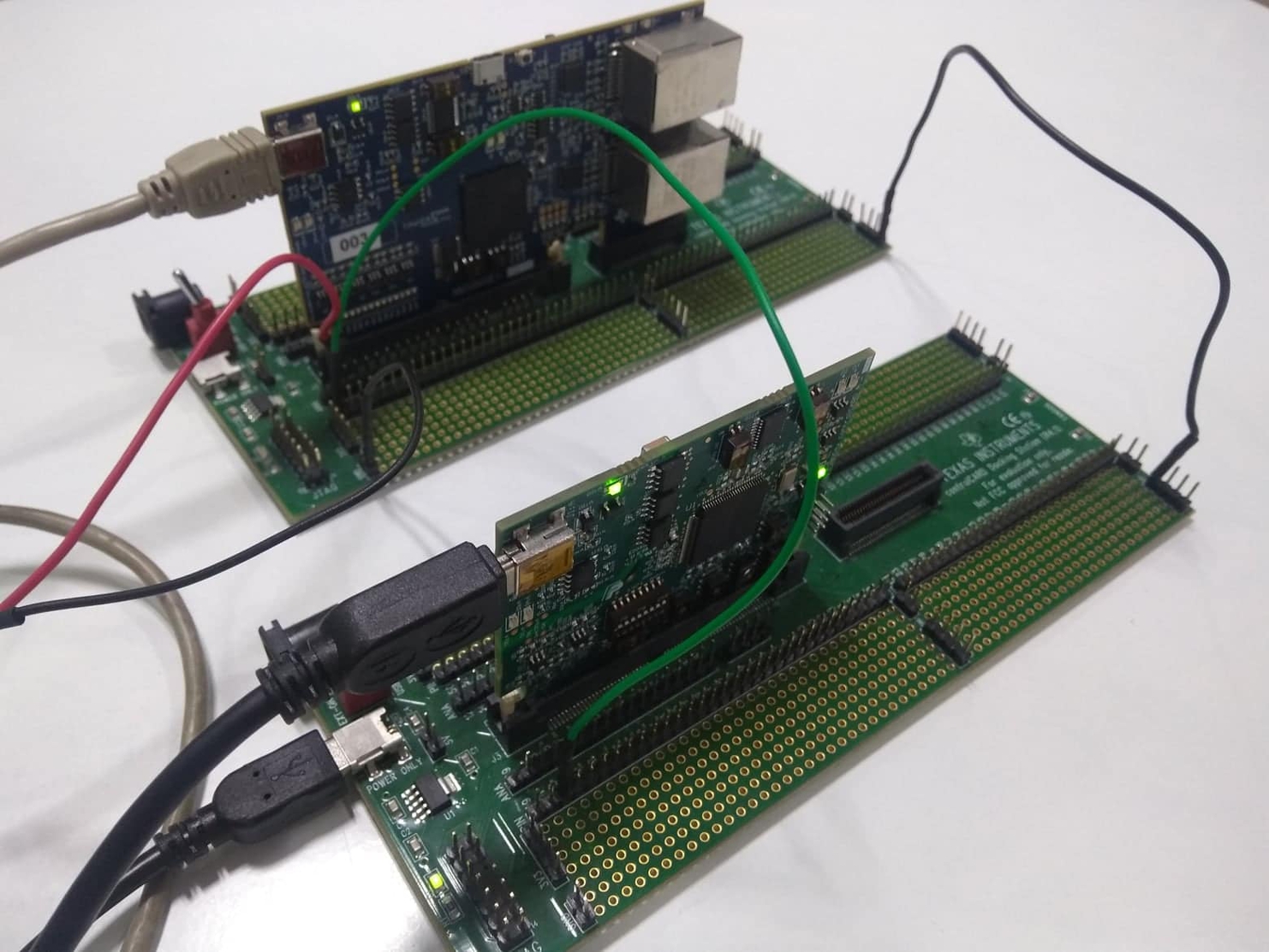
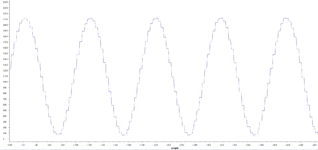
The proposed data transfer scheme based on HRCAP can be utilized for board-to-board communications across an isolation barrier and even for direct communication (without isolation). The experimental setup (shown in Figure 4) is used for validating the proposed technique, which consists of a direct single line connection between F2838x and F28004x controlCARD evaluation modules without isolation. The proposed scheme is tested for different frequencies and the performance metrics achieved with this experimental setup are measured in terms of ENOB and total transmission latency. Table 1 shows the performance metrics at different frequencies. You can refer to this table while choosing appropriate transmission PWM frequency based on your ENOB and latency requirements. The transmission latency consists of time taken by transmission PWM signal to travel to the receiver (time period) added with the time taken by decoding ISR at receiver to decode the data. Follow the directions included in the header section of the examples to add necessary watch variables to the expression window for evaluation. The snapshot of the expression windows of both transmitter and receiver CCS projects for manual data inspection mode are shown in Figure 5 and Figure 6. Also, the plot of decoded data at the receiver for ADC data transfer mode is shown in Figure 7, where the external sinusoid signal of 1 Khz is sampled at 25 Khz by transmitter and the transmission PWM frequency is 200 Khz. As the configured sampling frequency is less than the transmission frequency, the same data element is received multiple times at the receiver, which accounts for the zero slope lines in the plot.
Table 1. Performance Metrics at Different PWM Transmission Frequencies
| PWM Transmission Frequency | Effective Number of Bits (ENOB) | Transmission Latency |
|---|---|---|
| 100 KHz | 11.3 | 11.2 µs |
| 200 KHz | 11 | 6.2 µs |
| 500 KHz | 10.4 | 3.2 µs |
| 800 KHz | 9.83 | 2.45 µs |
NOTE
Table 1 shows the example results achieved with the discussed experimental setup. Introducing isolators or CMOS buffers/transceivers in the setup can provide dissimilar rise and fall times, which can need to comprehended and compensated for in the final system implementation .
 Figure 4. Test Setup for Cross Device Data Transfer
  Figure 5. Transmitter (F2838x) CCS Expression Window
  Figure 6. Receiver (F28004x) CCS Expression Window
  Figure 7. CCS Graph Plot of Decoded Data at Receiver (F28004x)