SPRADF4 December 2023 TMS320F280023C , TMS320F280025C , TMS320F280025C-Q1 , TMS320F280037C , TMS320F280037C-Q1 , TMS320F280039C , TMS320F280039C-Q1 , TMS320F280049C , TMS320F280049C-Q1 , TMS320F28377D , TMS320F28377D-EP , TMS320F28377D-Q1 , TMS320F28377S , TMS320F28377S-Q1 , TMS320F28379D , TMS320F28379D-Q1 , TMS320F28379S , TMS320F28P650DK
2 Basic CLB Implementation
The document, Implement Three-Phase Interleaved LLC on C2000™ Type-4 PWM, showcases using CLB for SR control. This application note discusses making the CLB logic more feasible for actual applications.
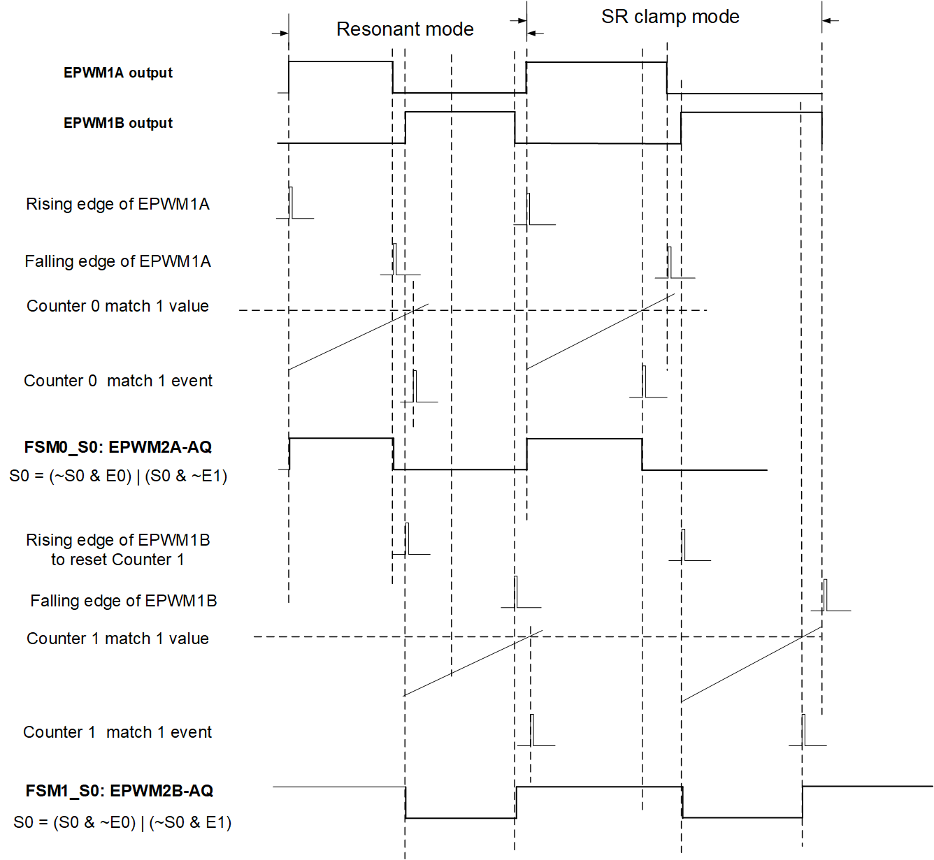
Figure 2-1 shows EPWM1 is selected as the primary-side PWM, EPWM2 is selected for SR PWM as the example, and the expected SR PWM configurations for resonant and SR clamp modes are included.
To achieve adjustable turn-on delay for SR PWM, the CLB module is not used to create the final SR PWM signals but the intermediate signal overriding the action qualifier (AQ) submodule output is used, meaning the addition of turn-on delay by the dead band (DB) submodule of the EPWM module is possible.
 Figure 2-1 CLB Configurations and SR Control
Logic
Figure 2-1 CLB Configurations and SR Control
LogicThe turn-on event is aligned with the rising edge of EPWM1A in example SR EPWM2A. The turn-off event follows the falling edge of EPWM1A during resonant mode or is limited by max on-time during SR clamp mode. Counter 0 is defined to start counting at the rising edge in the CLB and provide the match 1 event when the counter value reaches the predefined one (the predefined period corresponds to half of the resonant period). Users can utilize a look-up table (LUT) for ORing the falling edge and the match 1 event of Counter 0.
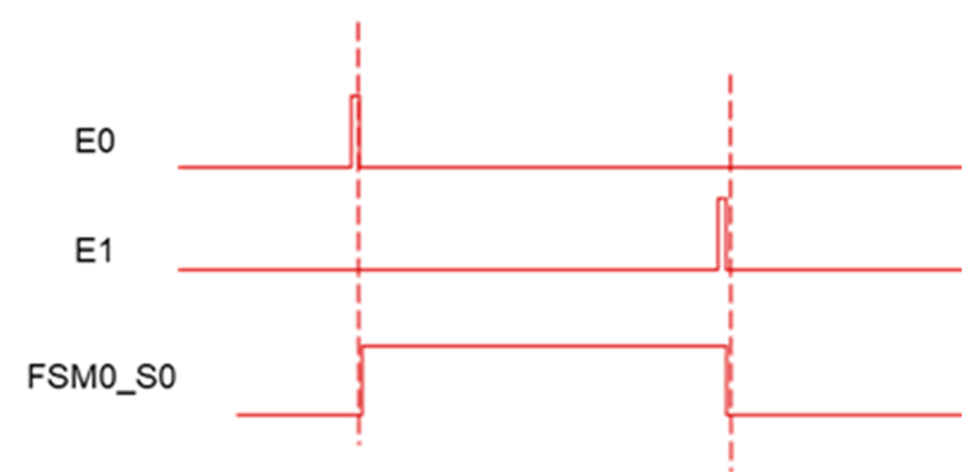
The finite state machine (FSM) is required for creating the expected logic for EPWM2A. In Figure 2-2, S0 is set to turn high at E0 and low at E1, with the rising edge of EPWM1A as an E0 event and LUT output as an E1 event. In Table 2-1, the Karnaugh map is created for S0 state.
 Figure 2-2 State Machine in the FSM
Block
Figure 2-2 State Machine in the FSM
Block| FSM0 S0 | ||||
|---|---|---|---|---|
| S0 E0E1 | 00 | 01 | 11 | 10 |
| 0 | 0 | 0 | 1 | 1 |
| 1 | 1 | 0 | 0 | 1 |
Based on the Karnaugh map, Equation 1 for FSM0_S0 is deducible as:
In Table 2-2, using FSM0_S0 to override the module output of EPWM2A is possible by assigning FSM0_S0 to output 4 of the CLB2 module directly with the CLB multiplexer output enable register CLB_OUT_EN. In the Table 2-2 example, the CLB2 module is selected for EPWM2 for the reasons explained in this section.
| CLB2 | |||
|---|---|---|---|
| CLB2 | CLB2_OUT0_0 | PWMA | EPWM2 |
| CLB2 | CLB2_OUT1_0 | PWMA_OE | EPWM2 |
| CLB2 | CLB2_OUT2_0 | PWMB | EPWM2 |
| CLB2 | CLB2_OUT3_0 | PWMB_OE | EPWM2 |
| CLB2 | CLB2_OUT4_0 | AQ_PWMA | EPWM2 |
| CLB2 | CLB2_OUT5_0 | AQ_PWMB | EPWM2 |
| CLB2 | CLB2_OUT6_0 | AQ_PWMA | EPWM2 |
| CLB2 | CLB2_OUT7_0 | AQ_PWMB | EPWM2 |
EPWM2B differs regarding FSM configurations because EPWM2B creates the AQ module output with the reverse polarity of EPWM1B (explained further in Section 3). Similarly, CLB2_OUT5 is activated to select FSM1_S0 as the AQ module output for EPWM2B.
Using the same method, the Equation 2 for FSM1_S0 is:
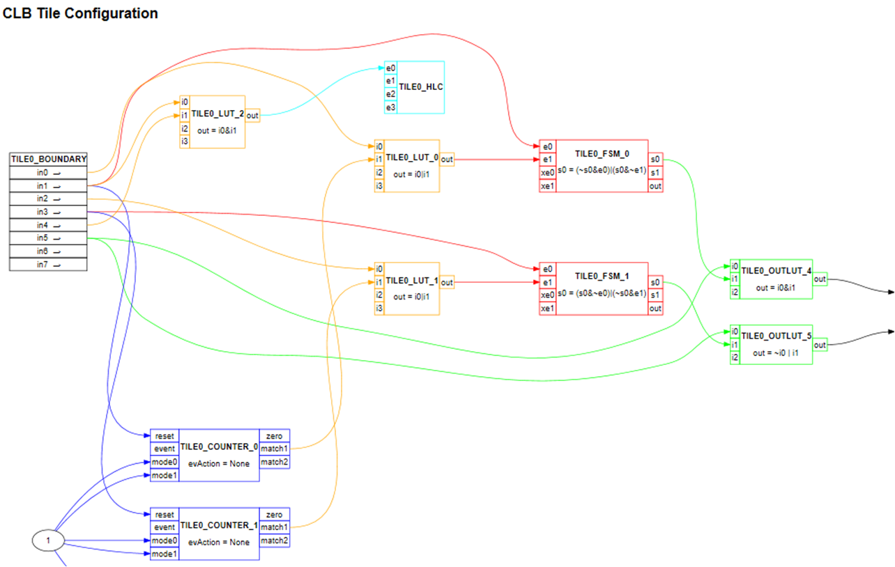
Alternatively, the CLB configuration diagram in Figure 2-3 is configurable to where IN0~IN4 refers to the falling edges of EPWM1A and EPWM1B and the rising edges of EPWM1B and EPWM1A. Additionally, IN5 turns the SR on and off (explained further in Section 5).
 Figure 2-3 CLB Configuration Diagram