SPRUIL8B May 2019 – May 2020 TMS320F28384D , TMS320F28384S , TMS320F28386D , TMS320F28386S , TMS320F28388D , TMS320F28388S
6 Hardware References
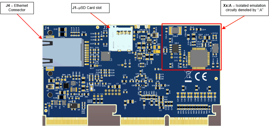
 Figure 5. Key Components on the controlCARD - Back
 Table 2. Hardware Connections
| Connectors | |
|---|---|
| J1:A | Emulation/UART connector - USB mini A connector used to provide XDS100v2 emulation and USB-to-UART (SCI) communication through FTDI logic. S1:A determines which connections are enabled to the MCU. |
| J1 | microSD card slot – connects to MCU via SPI |
| J2 | FSI Header |
| J3 | USB connector – USB micro AB connector supports USB 2.0 host/device |
| J4 | Ethernet connector – RJ45 connector |
| J5 | EtherCAT P0 – RJ45 connector |
| J6 | EtherCAT P1 – RJ45 connector |
| LEDs | |
|---|---|
| D2:A | Turns on when ISO JTAG logic is powered on (green) |
| D3:A | JTAG/UART RX toggle indicator (blue) |
| D4:A | JTAG/UART TX toggle indicator (blue) |
| D1 | Controlled by GPIO–31 with negative logic (red) |
| D2 | Controlled by GPIO–34 with negative logic (red) |
| D5 | Turns on when the controlCARD is powered ON (green) |
| D7 | Controlled by GPIO–145, EtherCAT Error LED (red) |
| D8 | Controlled by GPIO–146, EtherCAT Run LED (green) |
| Resistors and Capacitors | |
|---|---|
| R47, R48 | Alternate Reference Configuration Resistors: These resistors allow the user to choose whether the alternate reference for the ADCs will be given by:
|
| C16-C27, C32-C43 | Optional RC input filter for all ADC inputs |
| Switches | |
|---|---|
| S1:A | Isolated emulation and UART communication enable switches: |
S1:A Position 1 – JTAG Enable:
|
|
|
S1:A Position 2 – ISO UART communication enable:
|
|
| S1 | Reset switch: Switch connected to the XRSn line of the F28388D. Pressing this button will pull the device reset low. |
| S2 | Boot Mode Switch:Controls the Boot Options of the F2838x device, seeTable 3. For a full description see the device datasheet. |
| S3 | ADC VREFHI Control Switch for ADC modules A & B: |
S3 Position 1 (upper switch) – VREFHI Control Switch for ADC module A:
|
|
S3 Position 2 (lower switch) – VREFHI Control Switch for ADC module B:
|
|
| S4 | ADC VREFHI Control Switch for ADC modules C & D: |
S4 position 1 (upper switch) – VREFHI Control Switch for ADC module C:
|
|
S4Position 2 (lower switch) – VREFHI Control Switch for ADC module D:
|
|
| Test Points | |
|---|---|
| TP1:A | Emulator 5.0 V input: This power domain is isolated from the other 5.0V domain. |
| TP2:A | Emulator 3.3 V input: This power domain is isolated from the other 3.3 V domains. |
| TP3:A | Emulator ground |
| TP1 | ERRORSTS of F2838xD device |
| TP2 | XRSn of F2838xD device: Connected to the under-voltage outputs from both the 1.2 V and 3.3 V voltage supervisors. |
| TP3 | Over-voltage output: Connected to the over-voltage outputs from both the 1.2 V and 3.3 V voltage supervisors. |
| TP4 | P0 PHY clock source |
| TP5 | P1 PHY clock source |
| TP6 | F2838xD clock source |
| TP7 | HSEC 5.0 V input: 5.0 V input provided to the 3.3 V voltage regulator to create the unfiltered 3.3 V power. |
| TP8 | Filtered 3.3 V: Provides power to the F2838xD device. |
| TP9 | Filtered 1.2 V: Provides power to the F2838xD device. |
| TP10 | Device Ground |
NOTE
On the front of the controlCARD test points are indicated by their TPx number.
On the back of the controlCARD test points are indicated by their signal.
Table 3. S2, Bootmode Selection Table
| Mode | Switch Position 1 (GPIO-84) | Switch Position 2 (GPIO-72) | Boot From |
|---|---|---|---|
| 00 | 0 (right) | 0 (right) | Parallel I/O |
| 01 | 1 (left) | 0 (right) | SCI/Wait Boot |
| 02 | 0 (right) | 1 (left) | CAN |
| 03 | 1 (left) | 1 (left) | Flash/USB |
NOTE
S2 pulls the connected pin to a logic 0 when 'closed'. The 'ON' position of the switch indicates the 'closed' status of the switch NOT the logic level.
- S2 'ON' = Logic 0
- S2 'OFF' = Logic1
