SSZT583 november 2018 TPS62821 , TPS62822 , TPS62823 , TPS62824A , TPS62825 , TPS62825A , TPS62826 , TPS62826A , TPS62827 , TPS62827A

If you’re looking to power a space-constrained, high-power-density, thermally critical application, high-efficiency converters in tiny quad flat no-lead (QFN) packages offer great performance value. But you might ask yourself, when you test and debug your prototype boards, will you be able to handle those minuscule packages in your lab? Will you need special equipment or soldering talent?
No need to worry – it’s much easier than you think! Our lab experts have some hands-on tips and tricks for you.
First, make sure that your board is completely dry – otherwise there’s a risk of printed circuit board (PCB) delamination. Uniformly heat up the board from the bottom using a ceramic hot plate set at ~150°C (you can safely go up to 200°C for larger PCBs with eight layers or more).
To reach the right local soldering temperature, point a hot-air nozzle toward the integrated circuit (IC) landing position on the PCB. Since the IC package temperature should not exceed 260°C per TI specifications, be careful to limit the hot-air temperature.
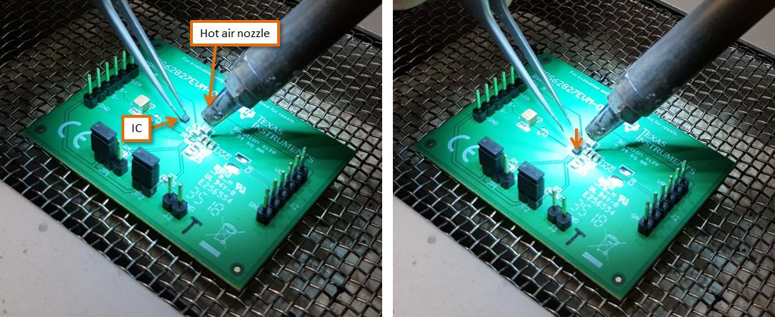
Once you’ve reached a stable temperature, apply the flux and distribute the solder evenly on the PCB pads (for such small packages, we use lead-free, 0.2-mm solder wire). Hold the IC with tweezers a few millimeters away from the landing pads during the PCB pad pre-tinning process. When the solder is molten on the pads, stop the airflow and drop the IC on the PCB pads (see Figure 1). The IC will self-align to the PCB pads as long as the solder is liquid. Carefully blowing some hot air again will help support the alignment.
 Figure 1 Keeping the IC above the
Landing Pads During the Pre-tinning Process (a); Dropping the IC on the PCB Pads
Once the Solder Is Molten and Carefully Blowing Hot Air to Support the Alignment
(b)
Figure 1 Keeping the IC above the
Landing Pads During the Pre-tinning Process (a); Dropping the IC on the PCB Pads
Once the Solder Is Molten and Carefully Blowing Hot Air to Support the Alignment
(b)Try to work as quickly as possible to avoid using up the flux and having the solder oxidize before you’ve properly placed the IC. Of course, pay attention to elementary precautions like working in an electrostatic discharge-safe environment.
That’s it!
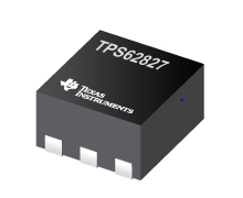
When you start working on your next thermally critical design using our new TPS62827, a 2- to 4-A high-efficiency buck converter in a 1.5-mm-by-1.5-mm QFN package, also check out the data sheet, which has specific guidance on how to properly lay out the PCB land pattern, solder mask and solder stencil for this package. In addition, the application note “QFN and SON PCB Attachment” gives a detailed overview of the essentials for ensuring the smooth manufacturability of your board.