SSZT658 july 2018 TPS7A37 , TPS7B7702-Q1
In most low-dropout regulators (LDOs), current flow is like one-way street – go in the wrong direction and major problems can occur! Reverse current is current that flows from VOUT to VIN instead of from VIN to VOUT. This current usually traverses through the body diode of the LDO instead of the normal conducting channel, and has the potential to cause long-term reliability problems or even destroy the device.
There are three main components to an LDO (see Figure 1): the bandgap reference, error amplifier and pass field-effect transistor (FET). The pass FET conducts current, as any normal FET, between the source and the drain in a typical application. The doped region used to create the body of the FET, called the bulk, is tied to the source; this reduces the amount of threshold voltage change.
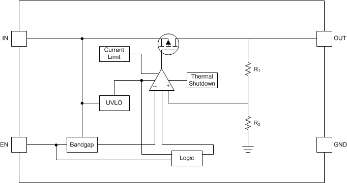 Figure 1 LDO Functional Block Diagram
One drawback of tying the bulk together with the source is that a parasitic body diode forms in the FET, as shown in Figure 2. This parasitic diode is called the body diode. In this configuration, the body diode can turn on when the output exceeds the input voltage plus the VFB of the parasitic diode. Reverse current flow through this diode can cause device damage through device heating, electromigration or latch-up events.
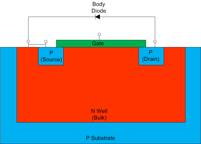 Figure 2 Cross-sectional View of a P-channel Metal-oxide Semiconductor (PMOS) FET
When designing your LDO, it is important to consider reverse current and how to prevent it. In this post, I’ll cover two ways of preventing reverse current at the application level and two ways during the integrated circuit (IC) design process.
There are four common methods for preventing reverse current flow, two at the application level and two during design.
Use a Schottky Diode
 Figure 3 Preventing Reverse Current Using a Schottky Diode
Use a Diode before the LDO
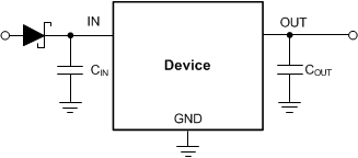 Figure 4 Reverse Current Prevention Using a Diode before the LDO
Use a Second FET
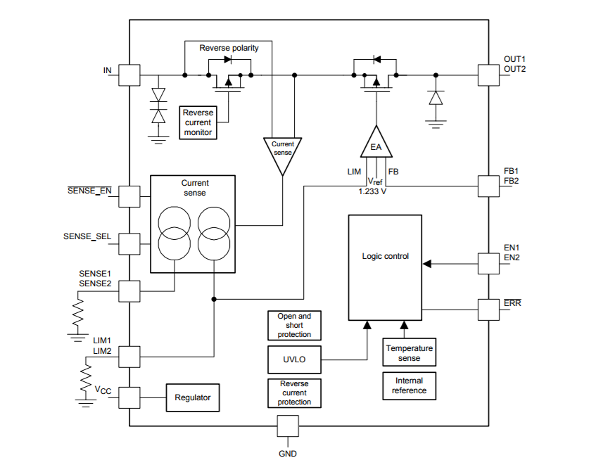 Figure 5 Back-to-back FETs to Prevent Reverse Current
Connect the Bulk of the MOSFET to GND
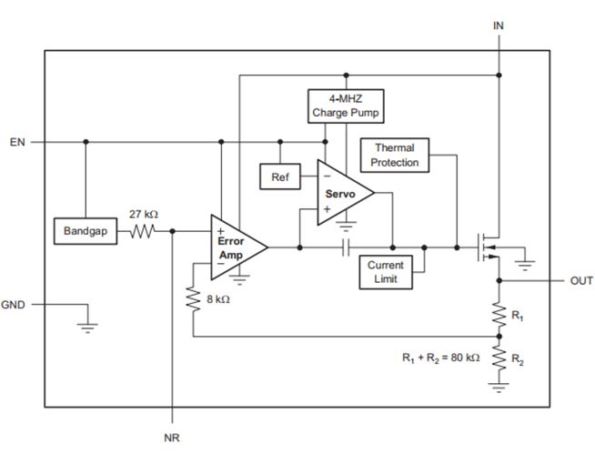 Figure 6 Connecting the Bulk of the FET to GND