SSZTAU6 september 2016 LM5017 , TPS5430
It is common knowledge in the DC/DC converter domain that a buck converter or regulator integrated circuit (IC), such as the LM5017 family, can create a negative VOUT from a positive VIN. At first glance, the schematic of an inverting buck-boost converter using a buck regulator IC looks deceivingly similar to a buck converter (Figure 1a and 1c). But there are important differences in the two circuits, both in terms of voltage and current levels, switching-current flow, and layout.
I discussed the differences between VIN range, VOUT range and available output current IOUT max in an earlier blog post. The difference in layout arising from the difference in switching-current flow paths of an inverting buck-boost converter and a buck converter – although critical – is not as well understood.
Figure 1 illustrates the difference in switching-current flow in a buck converter and an inverting buck-boost converter. In the buck converter (Figure 1a and 1b), the input loop – comprising the input capacitor CIN, high-side switch QH and synchronous rectifier QL, carries high di/dt switching current. The output loop, comprising the synchronous rectifier QL, inductor L1 and output capacitor COUT, has a relatively continuous current. Thus, while optimizing the input-current loop area is critical, it’s not as important to optimize the output-current loop area.
 Figure 1 Switching-current Flow in a
Buck Converter (a, B); and an Inverting Buck-boost Converter (C, D)
Figure 1 Switching-current Flow in a
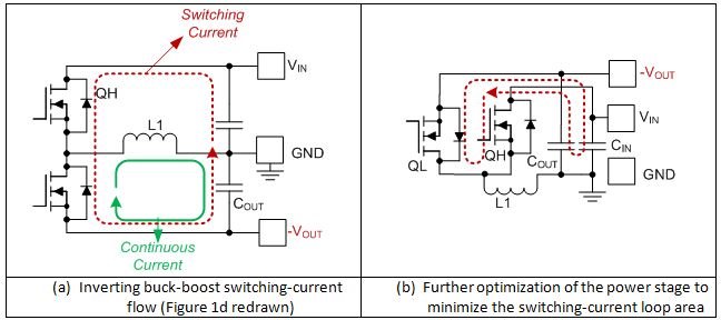
Buck Converter (a, B); and an Inverting Buck-boost Converter (C, D)The input- and output-current loops in an inverting buck-boost converter comprise the same elements as those in a buck converter (Figure 1c and 1d). The input loop has the input capacitor CIN, control FET QH and synchronous rectifier QL. The output-current loop consists of the synchronous rectifier QL, the filter inductor L1 and the output capacitor COUT. In an inverting buck-boost converter, however, both the input- and output-current loops carry high di/dt switching current because the filter inductor switches from CIN to COUT between the switching subintervals.
Because of the similarity in the buck and inverting schematics, the difference in switching-current paths often gets overlooked, and many inverting buck-boost designs and layouts are done just as they are for a buck converter, with only the input-current loop optimized for a small loop area. The buck to inverting buck-boost transition is often treated as a mere reconnection of VOUT and ground pins. But this approach fails to consider that the different current flows in a simple buck and an inverting buck-boost converter (using the same regulator IC) result in these issues:
- The switching-current path shown
in Figure 1c and 1d can have significant parasitic inductance, causing
higher spikes on the switch node with these adverse consequences:
- Higher electromagnetic interference (EMI) and noise as a result of switching current flowing through a non-optimized current loop.
- In the inverting buck-boost configuration, the MOSFETs see a higher spike voltage on top of the |VIN + VOUT| voltage.
- The switching current through the output capacitor has higher root mean square (RMS) (heating) content than in a buck converter for the same inductor current. The discontinuous current in the output capacitor also results in higher output ripple. Therefore, designers must keep these higher ripple currents in mind during output capacitor selection to satisfy both the VOUT ripple and IRMS current rating. Figure 2 compares the output capacitor ripple current in a buck and an inverting buck-boost converter.
 Figure 2 The Ripple Current in the
Output Filter Capacitor of a Buck Converter (a, B) Is Small, as the Inductor Is
Always Connected to the Output Node. the Ripple Current in the Output Filter
Capacitor of an Inverting Buck-boost Converter (C, D) Is Much Higher Due to the
Discontinuous Nature of Current Flowing through the Output Capacitor.
Figure 2 The Ripple Current in the
Output Filter Capacitor of a Buck Converter (a, B) Is Small, as the Inductor Is
Always Connected to the Output Node. the Ripple Current in the Output Filter
Capacitor of an Inverting Buck-boost Converter (C, D) Is Much Higher Due to the
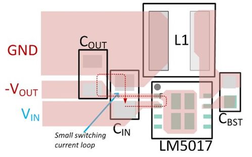
Discontinuous Nature of Current Flowing through the Output Capacitor.Figure 3 shows how to optimize an inverting buck-boost power stage to achieve lower di/dt input and output loops. Figure 4 shows an example inverting buck-boost power-stage layout using the LM5017, a 100V synchronous buck regulator.

 Figure 3 Optimization of Power-stage
Components to Minimize Switching-current Loop Area (a) Identifying Current Loops
(b) Minimizing Current Loops
 Figure 4 An Example Layout of an
Inverting Buck-boost Converter Based on the LM5017 Synchronous Buck
Regulator
Figure 4 An Example Layout of an
Inverting Buck-boost Converter Based on the LM5017 Synchronous Buck
RegulatorConclusion
Additional Resources
- Read the Analog Applications Journal article, “Using a buck converter in an inverting buck-boost topology.”
- Download the “Using the TPS5430 as an Inverting Buck-Boost Converter” application report.