How to Use Slew Rate for EMI Control
Many industrial and automotive applications use the synchronous buck converter power-supply topology; these applications also require low conducted and radiated emissions to ensure that the power supply does not interfere with other equipment sharing the same bus (input voltage [VIN]). For example, in an automotive infotainment system, electromagnetic interference (EMI) could result in unwanted noise in the car stereo.
Figure 1 shows a synchronous buck-converter schematic, along with its switch-node waveform. The ringing on the peak of the switch-node waveform is a function of both the high-side MOSFET’s switching speed and the high-side and low-side MOSFETs and printed circuit boards (PCB) stray inductance and capacitance. The ringing on the switch-node waveform is unwanted because it can increase the voltage stress on the low-side MOSFET and generate EMI.
 Figure 1 Synchronous Buck
Converter
Figure 1 Synchronous Buck
ConverterTo determine the relationship between the switch-node ringing of the buck converter in Figure 1 and the EMI that it generates, I ran conducted emissions testing in accordance with Comité International Spécial des Perturbations Radioélectriques (CISPR) 25 Class 5. Figure 2 shows the results. The measured data shows that the buck converter’s conducted emissions exceed Class 5 limits by 15dBµV in the 30MHz-108MHz frequency range.
 Figure 2 CISPR 25 Class 5,
30MHz-108MHz, Buck Converter vIN = 12V, vOUT = 3.3V,
IOUT = 5A
Figure 2 CISPR 25 Class 5,
30MHz-108MHz, Buck Converter vIN = 12V, vOUT = 3.3V,
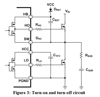
IOUT = 5AThe first step to lower the EMI is to reduce the switch-node ringing. There are several methods: the first is to slow down the MOSFET’s turn-on and turn-off time, which controls the rise and fall time of the switch node. You can do this by adding resistors in series (RHO and RLO) with the MOSFET’s gate leads; see Figure 3. A second method step is to add a snubber (RSUB and CSUB) from the switch node to ground. The snubber circuit dampens the parasitic inductances and capacitances during switching transitions.
An alternative to using the methods describe above to reduce switch-node ringing is to use the LM5140-Q1 automotive-qualified synchronous buck controller. One of the key features of the LM5140-Q1 is slew-rate control. By pinning out the driver’s source and sink leads, you can independently control the turn-on and turn-off time of both the high- and low-side MOSFETs.
During the period when the low-side bottom MOSFET is turning off and the high-side top MOSFET is turning on, the switch-node voltage rises from ground to VIN. If the high-side top MOSFET turn-on time is too fast, there is a high overshoot in the switch-node voltage during this transition. Increasing the RHO resistor decreases the drive current to the high-side MOSFET, slowing down this MOSFET’s turn-on time and helping reduce switch-node ringing. Note that slowing down the high-side MOSFET’s turn-off time will increase the switching losses. You will need to make a trade-off when selecting RHO between low EMI and the high-side MOSFET’s switching losses.
The losses in the low-side MOSFET include RDS(ON) losses, dead-time losses and losses in the MOSFET’s internal body diode. During the dead time (when the high- and low-side MOSFETs are turned off) the low-side MOSFET’s internal body diode conducts the inductor current. The MOSFET’s internal body diodes typically have a high forward-voltage drop, so there can be a significant reduction in efficiency. Reducing the time that the low-side MOSFET’s internal body diode conducts current improves efficiency.
Using slew-rate control, a resistor (ROL) can be inserted between the LM5140-Q1 driver output (LO pin) and the low-side MOSFETs gate to increase the time that it takes for the low-side MOSFET to turn-off. Slowing down the turn-off time decreases the dead time between the low- and high-side MOSFETs’ conduction, increasing buck-converter efficiency. When reducing the dead time for a synchronous buck, make sure that the high- and low-side MOSFETs never conduct at the same time.
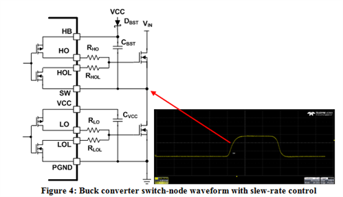
I modified the power supply shown in Figure 1 using the LM5140-Q1 controller (see Figure 4). Using slew-rate control optimizes the switch-node rise and fall time, eliminating switch-node ringing.
The next step is to run the CISPR 25 Class 5 conducted emissions. I chose these slew-rate control-resistor values: RHO = 10Ω, RHOL = 0Ω, RLO = 10Ω and RLOL = 10Ω. The resistors I selected for this application are a good startup point for any application where the output power is under 50W.
Figure 3 shows the results and summary of the conducted emissions testing.
 and with Slew-rate Control (b)") Figure 3 Slew-rate Control Comparison:
CISPR 25 Class 5, vIN = 12V, vOUT = 3.3V, IOUT
= 5A, without Slew-rate Control (a) and with Slew-rate Control (b)
Figure 3 Slew-rate Control Comparison:
CISPR 25 Class 5, vIN = 12V, vOUT = 3.3V, IOUT
= 5A, without Slew-rate Control (a) and with Slew-rate Control (b)The buck converter using the LM5140-Q1 with slew-rate control reduced conducted emissions by 21dBµV. It also provided better control of the switch-node rise and fall and eliminated the need for a snubber circuit, which adds circuit complexity and cost.
By picking the correct values of slew-rate control resistors, not only can you reduce EMI; you can also improve system efficiency.
See a live demonstration of the LM5140-Q1 buck converter in TI’s booth (No. 1617) at the Applied Power Electronics Conference (APEC), March 21-23 in Long Beach, California. Follow TI at www.ti.com/apec2016.
Additional Resources
- Watch the video “Engineer it: How to use slew rate control for EMI reduction.”
- See the LM5140-Q1 data sheet.
- Open the “LM5140-Q1 Evaluation Module User’s Guide.”
IMPORTANT NOTICE AND DISCLAIMER
TI PROVIDES TECHNICAL AND RELIABILITY DATA (INCLUDING DATASHEETS), DESIGN RESOURCES (INCLUDING REFERENCE DESIGNS), APPLICATION OR OTHER DESIGN ADVICE, WEB TOOLS, SAFETY INFORMATION, AND OTHER RESOURCES “AS IS” AND WITH ALL FAULTS, AND DISCLAIMS ALL WARRANTIES, EXPRESS AND IMPLIED, INCLUDING WITHOUT LIMITATION ANY IMPLIED WARRANTIES OF MERCHANTABILITY, FITNESS FOR A PARTICULAR PURPOSE OR NON-INFRINGEMENT OF THIRD PARTY INTELLECTUAL PROPERTY RIGHTS.
These resources are intended for skilled developers designing with TI products. You are solely responsible for (1) selecting the appropriate TI products for your application, (2) designing, validating and testing your application, and (3) ensuring your application meets applicable standards, and any other safety, security, or other requirements. These resources are subject to change without notice. TI grants you permission to use these resources only for development of an application that uses the TI products described in the resource. Other reproduction and display of these resources is prohibited. No license is granted to any other TI intellectual property right or to any third party intellectual property right. TI disclaims responsibility for, and you will fully indemnify TI and its representatives against, any claims, damages, costs, losses, and liabilities arising out of your use of these resources.
TI’s products are provided subject to TI’s Terms of Sale (www.ti.com/legal/termsofsale.html) or other applicable terms available either on ti.com or provided in conjunction with such TI products. TI’s provision of these resources does not expand or otherwise alter TI’s applicable warranties or warranty disclaimers for TI products.
Mailing Address: Texas Instruments, Post Office Box 655303, Dallas, Texas 75265
Copyright © 2023, Texas Instruments Incorporated