SSZTBO0 february 2016 LP2951
Can a low-dropout regulator (LDO) make a good load switch? Isn’t that like putting a round peg in a square hole? Well, yes, but an LDO can be a good choice if two or three of these conditions apply:
- The input voltage is >15V (this eliminates 80% of load switches).
- The output current is <1A (R-on is less critical).
- Every penny counts (The LDO may be less expensive than a load switch).
For an LDO to emulate a load switch, it must have a way to force operation in dropout mode. Adjustable LDOs have a feedback pin that enables you to put the device into dropout mode (full-on output). An LDO with field effect transistor pass element has low dropout voltage and low quiescent-current loss when in dropout mode. An LDO with bi-polar pass element that incorporates anti-saturation circuitry also has low dropout voltage and good quiescent-current loss when in dropout mode. There must be a way to turn the output off and on, LDOs with enable or shutdown pins have this feature.
As a bonus, LDOs have standard features only found in the best load switches, including:
- Current limiting.
- Rise-time control.
- Over-temperature shutdown.
Connecting the adjust pin to ground will force most adjustable LDOs to pass as much voltage to the output as possible. The voltage loss across the LDO is the same as the dropout-voltage specification in the data sheet. If you like, you can connect the adjust pin to a resistor to ground and a capacitor to VOUT, which will provide controlled-output slew-rate limiting. Slew rate ultimately sets the output rise time. Even with the feedback shorted to ground, the output rise time is still controlled by the output capacitance and the LDO current limit; however, this current usually varies with temperature and manufacturing processes. See the data sheet for the I-limit’s range.
For the aforementioned resistor and capacitor-feedback connection, the output rising slew rate (SR) is expressed as Equation 1:
Vref/(R*C) (1)
Vref is the LDO adjust-pin voltage and R and C are the feedback components. You can calculate the rise time using Equation 2:
[VIN–Vdo]*R*C/Vref (2)
Vdo is dropout voltage.
For the grounded feedback connection, use Equation 3 to calculate the output rising slew rate (in V/s):
[I-limit]/Cout (3)
The rise time is calculable as Equation 4:
[VIN–Vdo]*Cout/[I-limit] (4)
Figure 1 is a 24V load switch example using the inexpensive 100mA adjustable LP2951 LDO, which has a 1.25V feedback pin and an active-low enable pin compatible with most logic. R1 and C1 control the output rise time. I added a diode to the feedback pin to protect it from the capacitor current in cases of a VOUT instantaneous short.
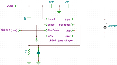 Figure 1 LP2951 Load Switch Schematic
 I measured the rise time in Figure 2 using 16.2k for R and 100nF for C. The calculated output rising slew rate was 1.25V/(16,200Ω*100nF) = 0.77V/ms. The measured value was 0.62V/ms.
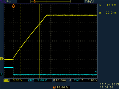 Figure 2 Output Rise Time
Waveform
Figure 2 Output Rise Time
WaveformThis slew-rate limiting tactic does have an unwanted side effect. As you can see in Figure 3, the first 870mV of rise time is much faster. This should not matter for most loads, however, especially 24V loads.
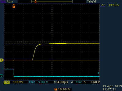 Figure 3 Initial Output Step
You could short feedback to ground and remove R1, C1 and D1 to reduce the component count. In this case, the rise time in Figure 4 is faster and is set by the current limit and output capacitance. Load current will steal current from the capacitor and slow the rise time. The rise slew rate (with a 40mA load) of 12.4V/ms suggests a current limit of 164mA (40mA into load and 124mA into the capacitor). Notice that there is still step up at the beginning of the rise.
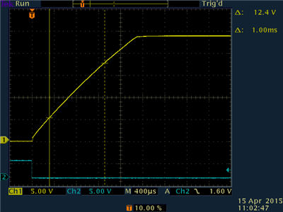 Figure 4 Output Rise Time Set by
Current Limit
Figure 4 Output Rise Time Set by
Current LimitFigure 5 is the DC output characteristic for VOUT vs. load current. The dropout (460mV voltage loss at 100mA) is acceptable for 24V systems. However, the current limit is not very well defined.
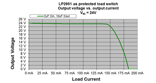 Figure 5 Output Voltage vs. Output
Current
Figure 5 Output Voltage vs. Output
CurrentFigure 6 is the ground current (quiescent current vs. output current). The PNP pass element has anti-saturation to keep the quiescent current in proportion to the load current.
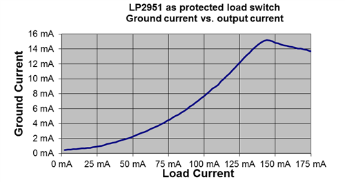 Figure 6 Quiescent Current
Lastly, Figure 7 is the output current vs. time for a shorted output case.
The device switches between current-limit mode and temperature-shutdown mode. Some LDOs can provide a steady lower output current that maintains the device at the shutdown temperature.
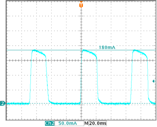 Figure 7 Short Circuit Current vs.
Time
Figure 7 Short Circuit Current vs.
TimeWhile load switches are generally best at switching power to loads, there are occasions when an LDO would be a better fit. Thinking outside the box can provide creative solutions.