Motor Drive Forum Top FAQs Part 2: How to Estimate Motor Regeneration and VM Pumping
Motor regeneration is a common problem that occurs in motor-drive systems. Many designers have to select a motor supply voltage (VM) rating of twice the nominal level, which adds to the system cost. Fortunately, if you can first understand the pumping details, you can understand the necessary VM margin. In the first post in this series on frequently asked questions, Nicholas Oborny provided advice on how to read a motor driver datasheet. Today, I’ll continue the conversation by introducing a method for estimating the pumping level.
VM Pumping Waveform
Figure 1 shows a typical VM pumping waveform caused by regeneration during a deceleration process. When the input PWM (pulse-width modulation) duty changed from 99% to 70%, the VM voltage was pumping from 24V to 32V. (Tested on TI motor driver device DRV8840, a 5A Brushed DC Motor Driver.)
 Figure 1 Regeneration and VM Pumping
Pumping Mechanism
We need some DC/DC power management background here to understand the pumping mechanism. So, let’s look at how a typical buck-boost circuit works; see Figure 2. What’s interesting is that during PWM, driving a motor with an H bridge, you have the buck and boost process together. As shown in Figure 3, during the PWM’s driving time, it’s a typical buck circuit. In Figure 4, the back electromotive force (EMF) is acting as the boost source during the PWM’s off time.
 Figure 2 Buck and Boost
Circuits
Figure 2 Buck and Boost
Circuits Figure 3 Buck Topology
 Figure 4 Boost Topology
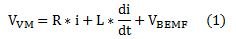
The running model of the brushed DC motor can be shown as equation Equation 1.
In normal driving conditions with a PWM duty cycle = D, the motor will run at a speed driven by a voltage VDRV as shown in equation Equation 2.

Based on Equation 1, we should have

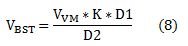
The boost effect will give the VBST as

From Equation 2, Equation 3, Equation 4, we can get

So, there is no VM pumping in a normal running condition.
When the PWM duty cycle is reduced from D1 to D2, just before the reducing point, we have

Just after the reducing of duty, the speed of the motor can’t change suddenly, so the VBST is based on the new duty cycle D2 as

From Equation 6, Equation 7, we can get
When K*D1/D2 > 1, we get
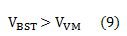
VBST will be higher than VVM and causing a pumping effect. Assuming that K is close to 1, any time you reduce the duty cycle with D2 < D1, VM pumping will occur. For example, if you go from 100% to 50%, VBST = 2*VM. And if you go from 90% to 30%, there will be 3x higher pumping voltage seen from VM.
Pumping Tests
In practice, VM pumping may not be seen as high as estimated by the above Equation 8, because the power supply and VM caps will have sinking ability which helps to reduce the pumping level. To verify the estimating method, we add a diode Ts1 from the power supply to the VM, as shown in Figure 5, trying to get the pure pumping effect without power supply sinking.
 Figure 5 Pumping Voltage Tests
Figure 6 and Figure 7 show the test results. (Note: Some pumping voltage is over the VM spec of the DRV8840 datasheet; this is for test only. The device is never recommended to be used in over-spec conditions.)
 Figure 6 Tested Result and Calculated
Result
Figure 6 Tested Result and Calculated
Result Figure 7 Bar Plot of Results
") Figure 8 VM Pumping When PWM Reduces
from 100% to 50% (with Ts1 on Figure 5)
Figure 8 VM Pumping When PWM Reduces
from 100% to 50% (with Ts1 on Figure 5)Reducing Voltage Pumping
There are two ways to control VM pumping:
- Use fast decay. With DRV8840 in fast decay mode, the boost topology shown in Figure 4 is no longer present. The back EMF will always be
less than the VM voltage, and VM pumping will not occur at all. It will take a longer time to achieve the targeted speed, as shown in Figure 9.
 Figure 9 No VM Pumping with Fast Decay
 - Use a transient voltage suppressor (TVS) to clamp the VM pumping. If you choose the TVS with clamping voltage a little higher than the nominal VM rating and place it as Ts2, shown in Figure 5, it will clamp the VM pumping (see Figure 10). I used a 27V TVS and the VM pumping was effectively clamped at 29.6V. The TVS also functioned as dynamic braking so that
the motor has a quick deceleration process.
 Figure 10 Figure 9
Summary
In a motor deceleration process, VM pumping actually shows the kinetic energy transferring into electrical energy. Consider the below factors:
- The boost topology is a key factor as to why the back EMF can force current back to the VM supply, even when VBEMF < VVM.Fast decay will not cause VM pumping during the deceleration section, but it will take a longer time for the motor to slow down.
- A TVS clamping method or other dynamic braking method can be a good way to reduce VM pumping while keeping the fast deceleration rate.
Additional Resources
- Read more blog posts in this series on frequently asked questions from the forum.
- Download the DRV8840 datasheet.
IMPORTANT NOTICE AND DISCLAIMER
TI PROVIDES TECHNICAL AND RELIABILITY DATA (INCLUDING DATASHEETS), DESIGN RESOURCES (INCLUDING REFERENCE DESIGNS), APPLICATION OR OTHER DESIGN ADVICE, WEB TOOLS, SAFETY INFORMATION, AND OTHER RESOURCES “AS IS” AND WITH ALL FAULTS, AND DISCLAIMS ALL WARRANTIES, EXPRESS AND IMPLIED, INCLUDING WITHOUT LIMITATION ANY IMPLIED WARRANTIES OF MERCHANTABILITY, FITNESS FOR A PARTICULAR PURPOSE OR NON-INFRINGEMENT OF THIRD PARTY INTELLECTUAL PROPERTY RIGHTS.
These resources are intended for skilled developers designing with TI products. You are solely responsible for (1) selecting the appropriate TI products for your application, (2) designing, validating and testing your application, and (3) ensuring your application meets applicable standards, and any other safety, security, or other requirements. These resources are subject to change without notice. TI grants you permission to use these resources only for development of an application that uses the TI products described in the resource. Other reproduction and display of these resources is prohibited. No license is granted to any other TI intellectual property right or to any third party intellectual property right. TI disclaims responsibility for, and you will fully indemnify TI and its representatives against, any claims, damages, costs, losses, and liabilities arising out of your use of these resources.
TI’s products are provided subject to TI’s Terms of Sale (www.ti.com/legal/termsofsale.html) or other applicable terms available either on ti.com or provided in conjunction with such TI products. TI’s provision of these resources does not expand or otherwise alter TI’s applicable warranties or warranty disclaimers for TI products.
Mailing Address: Texas Instruments, Post Office Box 655303, Dallas, Texas 75265
Copyright © 2023, Texas Instruments Incorporated