SWRA640H December   2018  – May 2024 CC1310 , CC1312R , CC1314R10 , CC1350 , CC1352P , CC1352R , CC1354P10 , CC1354R10 , CC2620 , CC2630 , CC2640 , CC2640R2F , CC2640R2F-Q1 , CC2642R , CC2642R-Q1 , CC2650 , CC2652P , CC2652R , CC2652R7 , CC2652RB , CC2652RSIP , CC2674P10 , CC2674R10


  1.   1
  2.   Abstract
  3.   Trademarks
  4. Reference Design
    1. 1.1 Sub-1GHz LaunchPads
      1. 1.1.1 LAUNCHXL-CC1310
      2. 1.1.2 LAUNCHXL-CC1312R
    2. 1.2 2.4GHz LaunchPads
      1. 1.2.1 LAUNCHXL-CC2640R2
      2. 1.2.2 LAUNCHXL-CC26x2R
      3. 1.2.3 LP-CC26x1
    3. 1.3 Dual-Band LaunchPads
      1. 1.3.1 LAUNCHXL-CC1350EU/US
      2. 1.3.2 LAUNCHXL-CC1350-4
      3. 1.3.3 LAUNCHXL-CC1352R
      4. 1.3.4 LAUNCHXL-CC1352P1
      5. 1.3.5 LAUNCHXL-CC1352P-2
      6. 1.3.6 LAUNCHXL-CC1352P-4
      7. 1.3.7 LP-CC1352P7-1
      8. 1.3.8 LP-CC1352P7-4
      9. 1.3.9 LP-EM-CC1354P10-6
    4. 1.4 Reference Design Overview
  5. Front-End Configurations
    1. 2.1 Overview of Front-end Configurations
    2. 2.2 Configuring the Front-End Mode
    3. 2.3 CC13xx Single-Ended Mode
      1. 2.3.1 Single-Ended Modes
      2. 2.3.2 Single-Ended TX-Only
      3. 2.3.3 Single-Ended RX-Only
      4. 2.3.4 Single-Ended Modes - 2.4GHz
    4. 2.4 CC26xx Single-End Mode
  6. Schematic
    1. 3.1 Schematic Overview
      1. 3.1.1 24/48MHz Crystal
      2. 3.1.2 32.768kHz Crystal
      3. 3.1.3 Balun
      4. 3.1.4 Filter
      5. 3.1.5 RX_TX Pin
      6. 3.1.6 Decoupling Capacitors
      7. 3.1.7 Antenna Components
      8. 3.1.8 RF Shield
      9. 3.1.9 I/O Pins Drive Strength
    2. 3.2 Bootloader Pins
    3. 3.3 AUX Pins
      1. 3.3.1 Reference
      2. 3.3.2 CC26x2/CC13x2 AUX Pins
      3. 3.3.3 CC26x0/CC13x0 AUX Pins
    4. 3.4 JTAG Pins
  7. PCB Layout
    1. 4.1  Board Stack-Up
    2. 4.2  Balun - Sub-1GHz
    3. 4.3  Balun - 2.4GHz
      1. 4.3.1 Recommended Layout and Considerations for 20dBm
    4. 4.4  LC Filter
    5. 4.5  Decoupling Capacitors
    6. 4.6  Placement of Crystal Load Capacitors
    7. 4.7  Current Return Path
    8. 4.8  DC/DC Regulator
    9. 4.9  Antenna Matching Components
    10. 4.10 Transmission Lines
    11. 4.11 Electromagnetic Simulation
  8. Antenna
    1. 5.1 Single-Band Antenna
    2. 5.2 Dual-Band Antenna
      1. 5.2.1 Dual-Band Antenna Match Example: 863-928 MHz and 2.4 GHz
      2. 5.2.2 Dual-Band Antenna Match: 433-510MHz and 2.4GHz
  9. Crystal Tuning
    1. 6.1 CC13xx/CC26xx Crystal Oscillators
    2. 6.2 Crystal Selection
    3. 6.3 Tuning the LF Crystal Oscillator
    4. 6.4 Tuning the HF Oscillator
  10. TCXO Support
    1. 7.1 Hardware
    2. 7.2 Software
    3. 7.3 Example: Usage of TCXO on CC1312R Launchpad
  11. Integrated Passive Component (IPC)
  12. Optimum Load Impedance
  13. 10PA Table
  14. 11Power Supply Configuration
    1. 11.1 Introduction
    2. 11.2 DC/DC Converter Mode
    3. 11.3 Global LDO Mode
    4. 11.4 External Regulator Mode
  15. 12Board Bring-Up
    1. 12.1 Power On
    2. 12.2 RF Test: SmartRF Studio
    3. 12.3 RF Test: Conducted Measurements
      1. 12.3.1 Sensitivity
      2. 12.3.2 Output Power
    4. 12.4 Software Bring-Up
    5. 12.5 Hardware Troubleshooting
      1. 12.5.1 No Link: RF Settings
      2. 12.5.2 No Link: Frequency Offset
      3. 12.5.3 Poor Link: Antenna
      4. 12.5.4 Bluetooth Low Energy: Device Does Advertising But Cannot Connect
      5. 12.5.5 Poor Sensitivity: DCDC Layout
      6. 12.5.6 Poor Sensitivity: Background noise
      7. 12.5.7 High Sleep Power Consumption
  16. 13References
  17. 14Revision History

Current Return Path

There needs to be a solid ground plane from the capacitor ground pad back to the chip. Figure 4-6 illustrates this. In the bad example, notice the break in ground plane on layer 2 causing a longer return path while the good example has no breaks. Failure to follow this can lead to reduced RF performance and higher spurious emissions.
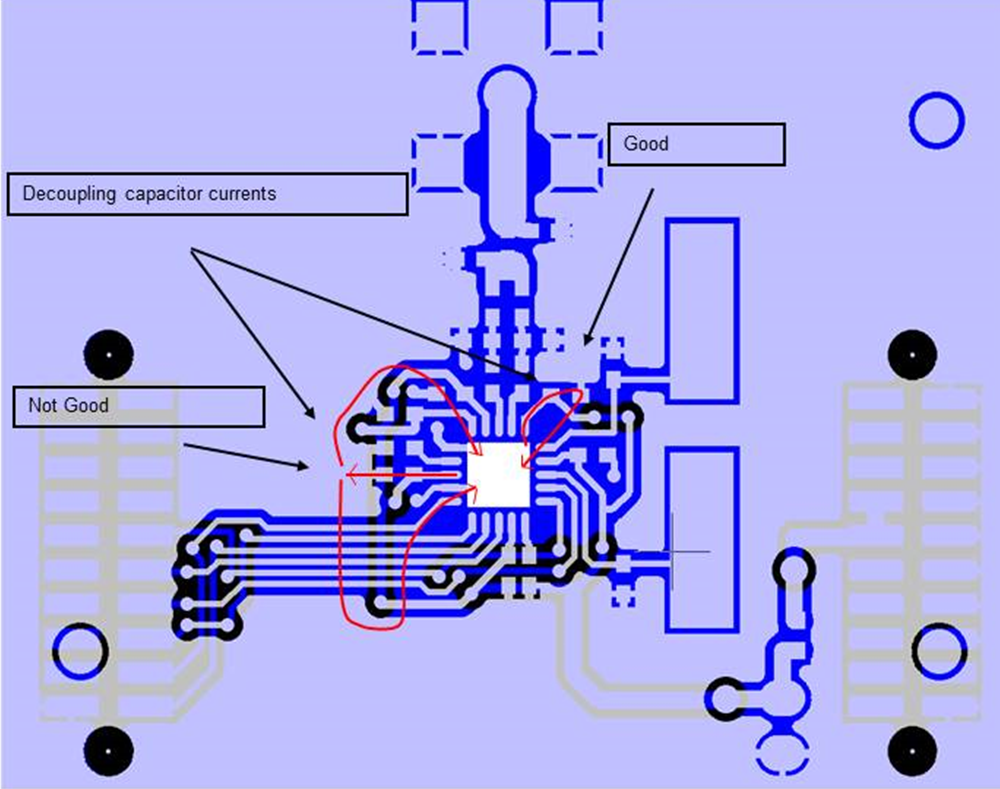
CC1354P10-6 Current Return Path Figure 4-6 Current Return Path