SWRA640H December   2018  – May 2024 CC1310 , CC1312R , CC1314R10 , CC1350 , CC1352P , CC1352R , CC1354P10 , CC1354R10 , CC2620 , CC2630 , CC2640 , CC2640R2F , CC2640R2F-Q1 , CC2642R , CC2642R-Q1 , CC2650 , CC2652P , CC2652R , CC2652R7 , CC2652RB , CC2652RSIP , CC2674P10 , CC2674R10


  1.   1
  2.   Abstract
  3.   Trademarks
  4. Reference Design
    1. 1.1 Sub-1GHz LaunchPads
      1. 1.1.1 LAUNCHXL-CC1310
      2. 1.1.2 LAUNCHXL-CC1312R
    2. 1.2 2.4GHz LaunchPads
      1. 1.2.1 LAUNCHXL-CC2640R2
      2. 1.2.2 LAUNCHXL-CC26x2R
      3. 1.2.3 LP-CC26x1
    3. 1.3 Dual-Band LaunchPads
      1. 1.3.1 LAUNCHXL-CC1350EU/US
      2. 1.3.2 LAUNCHXL-CC1350-4
      3. 1.3.3 LAUNCHXL-CC1352R
      4. 1.3.4 LAUNCHXL-CC1352P1
      5. 1.3.5 LAUNCHXL-CC1352P-2
      6. 1.3.6 LAUNCHXL-CC1352P-4
      7. 1.3.7 LP-CC1352P7-1
      8. 1.3.8 LP-CC1352P7-4
      9. 1.3.9 LP-EM-CC1354P10-6
    4. 1.4 Reference Design Overview
  5. Front-End Configurations
    1. 2.1 Overview of Front-end Configurations
    2. 2.2 Configuring the Front-End Mode
    3. 2.3 CC13xx Single-Ended Mode
      1. 2.3.1 Single-Ended Modes
      2. 2.3.2 Single-Ended TX-Only
      3. 2.3.3 Single-Ended RX-Only
      4. 2.3.4 Single-Ended Modes - 2.4GHz
    4. 2.4 CC26xx Single-End Mode
  6. Schematic
    1. 3.1 Schematic Overview
      1. 3.1.1 24/48MHz Crystal
      2. 3.1.2 32.768kHz Crystal
      3. 3.1.3 Balun
      4. 3.1.4 Filter
      5. 3.1.5 RX_TX Pin
      6. 3.1.6 Decoupling Capacitors
      7. 3.1.7 Antenna Components
      8. 3.1.8 RF Shield
      9. 3.1.9 I/O Pins Drive Strength
    2. 3.2 Bootloader Pins
    3. 3.3 AUX Pins
      1. 3.3.1 Reference
      2. 3.3.2 CC26x2/CC13x2 AUX Pins
      3. 3.3.3 CC26x0/CC13x0 AUX Pins
    4. 3.4 JTAG Pins
  7. PCB Layout
    1. 4.1  Board Stack-Up
    2. 4.2  Balun - Sub-1GHz
    3. 4.3  Balun - 2.4GHz
      1. 4.3.1 Recommended Layout and Considerations for 20dBm
    4. 4.4  LC Filter
    5. 4.5  Decoupling Capacitors
    6. 4.6  Placement of Crystal Load Capacitors
    7. 4.7  Current Return Path
    8. 4.8  DC/DC Regulator
    9. 4.9  Antenna Matching Components
    10. 4.10 Transmission Lines
    11. 4.11 Electromagnetic Simulation
  8. Antenna
    1. 5.1 Single-Band Antenna
    2. 5.2 Dual-Band Antenna
      1. 5.2.1 Dual-Band Antenna Match Example: 863-928 MHz and 2.4 GHz
      2. 5.2.2 Dual-Band Antenna Match: 433-510MHz and 2.4GHz
  9. Crystal Tuning
    1. 6.1 CC13xx/CC26xx Crystal Oscillators
    2. 6.2 Crystal Selection
    3. 6.3 Tuning the LF Crystal Oscillator
    4. 6.4 Tuning the HF Oscillator
  10. TCXO Support
    1. 7.1 Hardware
    2. 7.2 Software
    3. 7.3 Example: Usage of TCXO on CC1312R Launchpad
  11. Integrated Passive Component (IPC)
  12. Optimum Load Impedance
  13. 10PA Table
  14. 11Power Supply Configuration
    1. 11.1 Introduction
    2. 11.2 DC/DC Converter Mode
    3. 11.3 Global LDO Mode
    4. 11.4 External Regulator Mode
  15. 12Board Bring-Up
    1. 12.1 Power On
    2. 12.2 RF Test: SmartRF Studio
    3. 12.3 RF Test: Conducted Measurements
      1. 12.3.1 Sensitivity
      2. 12.3.2 Output Power
    4. 12.4 Software Bring-Up
    5. 12.5 Hardware Troubleshooting
      1. 12.5.1 No Link: RF Settings
      2. 12.5.2 No Link: Frequency Offset
      3. 12.5.3 Poor Link: Antenna
      4. 12.5.4 Bluetooth Low Energy: Device Does Advertising But Cannot Connect
      5. 12.5.5 Poor Sensitivity: DCDC Layout
      6. 12.5.6 Poor Sensitivity: Background noise
      7. 12.5.7 High Sleep Power Consumption
  16. 13References
  17. 14Revision History

Decoupling Capacitors

General rules for decoupling capacitors:

  • Ensure decoupling capacitors are on same layer as the active component for best results.
  • Route power into the decoupling capacitor and then into the active component.
  • Each decoupling capacitor should have a separate via to ground to minimize noise coupling (see Figure 4-5).
  • The decoupling capacitor should be placed close to the pin it is supposed decouple (see Figure 3-2).
  • The ground current return path between decoupling capacitor and chip should be short and direct (low impedance). For details, see Section 4.7.
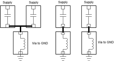
CC1354P10-6 Decoupling Capacitors and VIA to GroundFigure 4-5 Decoupling Capacitors and VIA to Ground

The right side of Figure 4-5 that uses separate vias to ground has less noise coupling.