SWRU612 December 2023 CC3300 , CC3301 , CC3301MOD , CC3351
- 1
- Abstract
- Trademarks
- 1Introduction
-
2Schematic Considerations
- 2.1 Schematic Reference Design
- 2.2 Power Supply
- 2.3 Clock Source
- 2.4 Radio Frequency (RF)
- 2.5 Digital Interfaces
- 3Layout Considerations
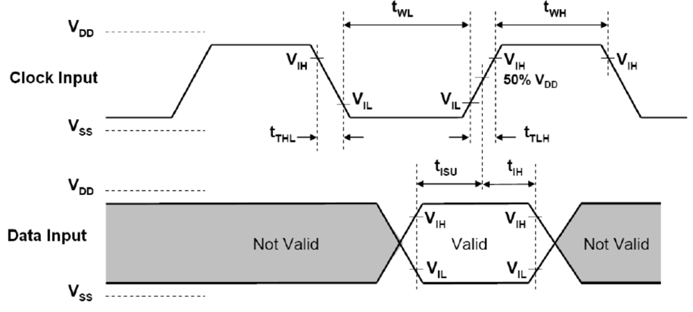
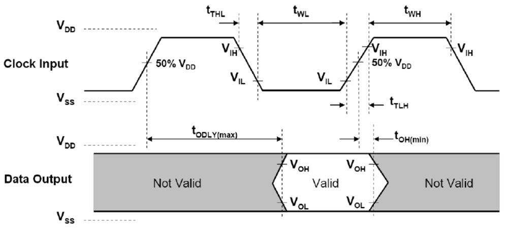
2.5.2.2 SDIO Timing Diagram - High Speed
 Figure 2-5 SDIO HS Input Timing
 Figure 2-6 SDIO HS Output Timing
Table 2-6 SDIO Timing Parameters - High
Speed
| Parameter | Description | MIN | MAX | Unit |
|---|---|---|---|---|
| fclock | Clock frequency, CLK | 52 | MHz | |
| tHigh | High Period | 7 | ns | |
| tLow | Low Period | 7 | ||
| tTLH | Rise time, CLK | 3 | ||
| tTHL | Fall time, CLK | 3 | ||
| tISU | Setup time, input valid before CLK ↑ | 6 | ||
| tIH | Hold time, input valid after CLK ↑ | 2 | ||
| tODLY | Delay time, CLK ↓ to output valid | 2 | 14 | |
| CL | Capacitive load on outputs | 15 | 40 |
pF |