Circuit to measure multiple redundant source currents with singled-ended signal
| Input | Output | Error | Supply | ||||||
|---|---|---|---|---|---|---|---|---|---|
| ILOAD Min | ILOAD Max | VCM | IOUT Min | IOUT Max | Bandwidth | ILOAD > 45 A | IDD | VS | Vee |
| 5A | 304A | 12V | 42.1µA | 1.6842mA | 400kHz | 2.1% maximum at full-scale range | N × (2.4mA + 750µA) + IOUT | 5V | GND (0V) |
Design Description
This circuit demonstrates how to convert a voltage-output, current-sense amplifier (CSA) into a current-output circuit using the Howland Current Pump method and operational amplifier (op amp). Furthermore, this circuit demonstrates how to design two separate circuits to measure two separate, but redundant supplies powering one load.

Design Notes
- The Getting Started with Current Sense Amplifiers video series introduces implementation, error sources, and advanced topics for using current sense amplifiers.
- Choose precision 0.1% resistors to limit gain error at higher currents.
- The output current (IOUT) is sourced from the VS supply, which adds to the IQ of the current sense amplifier.
- Use the VOUT versus IOUT curve ("claw-curve") of the CSA (INA240A3) to set the IOUT limit during maximum power. If a higher signal current is needed, then add an op amp buffer to the output of the current sense amplifier. A buffer on the output allows for smaller ROUT.
- For applications with higher bus voltages, simply substitute in a bidirectional current sense amplifier with a higher rated input voltage.
- The VOUT voltage is the input common-mode voltage (VCM) for the op amp.
- Offset errors can be calibrated out with one-point calibration given that a known sense current is applied and the circuit is operating in the linear region. Gain error calibration requires a two-point calibration.
- Include a small feed-forward capacitor (CSET) to increase BW and decrease VOUT settling time to a step response in current. Increasing CSET too much introduces gain peaking in the system gain curve, which results in output overshoot to a step response.
- Follow best practices for printed-circuit board (PCB) layout according to the data sheet: place the decoupling capacitor close to the VS pin, routing the input traces for IN+ and IN– as a differential pair, and so forth.
Design Steps
- Choose an available current-sense
amplifier (CSA) that meets the common-mode voltage requirement. For this design
the INA240A3 is selected.
- Note that choosing the most optimal CSA for the system requires balancing tradeoffs in CSA offset, CSA gain error, shunt resistor power rating and thus total circuit design could require multiple iterations to achieve the satisfactory error over the entire dynamic range of the load.
- Determine the maximum output current (ISET_100%) and maximum output swing (VO_ISYS_MAX) of the INA240A3. Use the output current vs output voltage curve in the data sheet. For this design, choose the maximum ISET to be 850 µA with a maximum output swing of {Vs – 0.2V} = 4.8V = VO_ISYS_MAX.
- Given the ADC full-scale range
(VADC_FSR = 1.8V), the number of sources to measure (N = 2), and
the maximum CSA output current when the source is at 100% power
(ISET_100% = 850µA), calculate the maximum allowable
ROUT which converts signal current to signal voltage for ADC. For
this design ROUT = 1020 Ω is selected.
- Using
the following system of equations, we can solve for the minimum allowable
RSET. For this design, RSET = 3610 Ω is selected.
- Using the following system of
equations, solve for the maximum allowable shunt resistor. For this design,
choose RSHUNT = 200 µΩ.
- Check that the common-mode voltage
(VCM) and output voltage (VO_TLV9061) of the TLV9061
are in the operational region when the circuit is sensing the minimum required
5% source current. The TLV9061 device is a rail-to-rail-input-output (RRIO) op
amp so it can operate with very small VCM and output voltages, but
AOL will vary. Testing conditions from the data sheet for CMRR
and AOL show that choosing VOUT_5% ≥ 40mV provides
sufficient AOL when circuit sensing minimum load current.
- If a lower operational VCM is needed, then consider providing
a small negative voltage source to the negative supply pin to extend the
range of the op amp or current-sense amplifier.
- If a lower operational VCM is needed, then consider providing
a small negative voltage source to the negative supply pin to extend the
range of the op amp or current-sense amplifier.
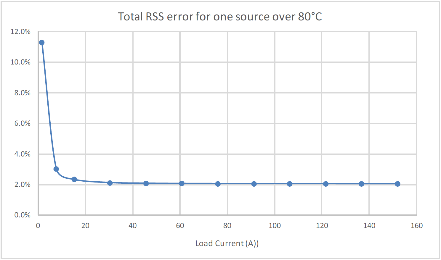
- Using the following equations,
calculate and tabulate the total, worst-case RSS error over the dynamic range of
the source.
- Plot the
total error as a function of load current
Design Simulations
DC Simulation Results
The following graph shows a linear output response for load currents from 5A to 304A.

AC Simulation Result – ILOAD to IOUT (VOUT) circuit gain

Design References
See Analog Engineer's Circuit Cookbooks for TI's comprehensive circuit library.
Getting Started with Current Sense Amplifiers video series
https://training.ti.com/getting-started-current-sense-amplifiers
Current Sense Amplifiers on TI.com
http://www.ti.com/amplifier-circuit/current-sense/products.html
Comprehensive Study of the Howland Current Pump
For direct support from TI Engineers use the E2E community
Design Featured Current Sense Amplifier
| INA240A3 | |
|---|---|
| VS | 2.7V to 5.5V (operational) |
| VCM | –4V to 80V |
| Swing to VS (VSP) | VS – 0.2V |
| VOS | ±25µV at 12V VCM |
| IQ_MAX | 2.4mV |
| IIB | 90µA at 12V |
| BW | 400kHz |
| # of channels | 1 |
| Body size (including pins) | 4mm × 3.91mm |
| www.ti.com/product/ina240 | |
Design Featured Operational Amplifier
| TLV9061 (TLV9061S is shutdown version) | |
| VS | 1.8V to 5.5V |
| VCM | (V–) – 0.1V < VCM < (V+) + 0.1V |
| CMRR | 103dB |
| AOL | 130dB |
| VOS | ±1.6mV maximum |
| IQ | 750µA maximum |
| IB (input bias current) | ± 0.5pA |
| GBP (gain bandwidth product) | 10MHz |
| # of channels | 1 (2 and 4 channel packages available) |
| Body size (including pins) | 0.80mm × 0.80mm |
| www.ti.com/product/tlv9061 | |
IMPORTANT NOTICE AND DISCLAIMER
TI PROVIDES TECHNICAL AND RELIABILITY DATA (INCLUDING DATASHEETS), DESIGN RESOURCES (INCLUDING REFERENCE DESIGNS), APPLICATION OR OTHER DESIGN ADVICE, WEB TOOLS, SAFETY INFORMATION, AND OTHER RESOURCES “AS IS” AND WITH ALL FAULTS, AND DISCLAIMS ALL WARRANTIES, EXPRESS AND IMPLIED, INCLUDING WITHOUT LIMITATION ANY IMPLIED WARRANTIES OF MERCHANTABILITY, FITNESS FOR A PARTICULAR PURPOSE OR NON-INFRINGEMENT OF THIRD PARTY INTELLECTUAL PROPERTY RIGHTS.
These resources are intended for skilled developers designing with TI products. You are solely responsible for (1) selecting the appropriate TI products for your application, (2) designing, validating and testing your application, and (3) ensuring your application meets applicable standards, and any other safety, security, or other requirements. These resources are subject to change without notice. TI grants you permission to use these resources only for development of an application that uses the TI products described in the resource. Other reproduction and display of these resources is prohibited. No license is granted to any other TI intellectual property right or to any third party intellectual property right. TI disclaims responsibility for, and you will fully indemnify TI and its representatives against, any claims, damages, costs, losses, and liabilities arising out of your use of these resources.
TI’s products are provided subject to TI’s Terms of Sale (www.ti.com/legal/termsofsale.html) or other applicable terms available either on ti.com or provided in conjunction with such TI products. TI’s provision of these resources does not expand or otherwise alter TI’s applicable warranties or warranty disclaimers for TI products.
Mailing Address: Texas Instruments, Post Office Box 655303, Dallas, Texas 75265
Copyright © 2023, Texas Instruments Incorporated
