-
UCC28782 Practical Design Guidelines
UCC28782 Practical Design Guidelines
Trademarks
All trademarks are the property of their respective owners.
1 Introduction
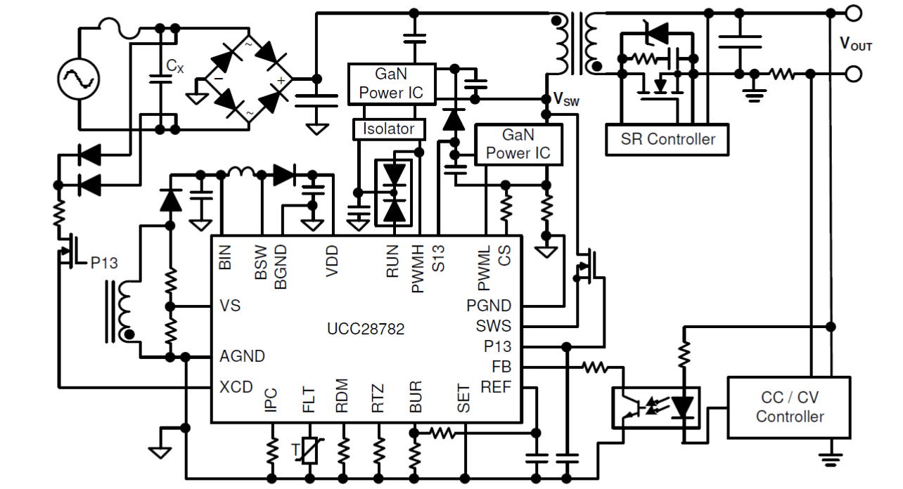
The UCC28782 is a transition-mode (TM) active clamp flyback (ACF) controller, equipped with advanced control schemes, to enable significant size reduction of passive components, for higher power density and higher average efficiency. The control law is optimized for Silicon (Si) and Gallium Nitride (GaN) power FETs in a half-bridge configuration and is capable of driving high-frequency AC/DC converters up to 1.5 MHz. The zero voltage switching (ZVS) control of the UCC28782 is capable of auto-tuning the on-time of a high-side clamp switch (QH) by using a unique loss less ZVS sensing network connected between the switch-node voltage (VSW) and SWS pin. The ACF controller is designed to adaptively achieve targeted full-ZVS or partial-ZVS conditions for the low-side main switch (QL) with minimum circulating energy over wide operating conditions. Auto-tuning eliminates the risk of losing ZVS due to component tolerance, input/output voltage changes, and temperature variations, since the QH on-time is corrected cycle-by-cycle.
 Figure 1-1 Simplified Type Circuit
2 Control Law across Entire Load Range
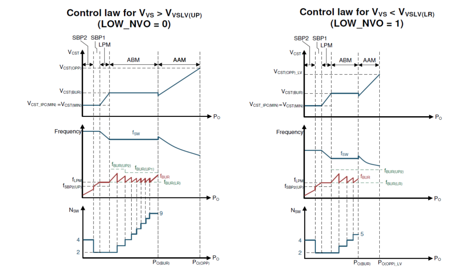
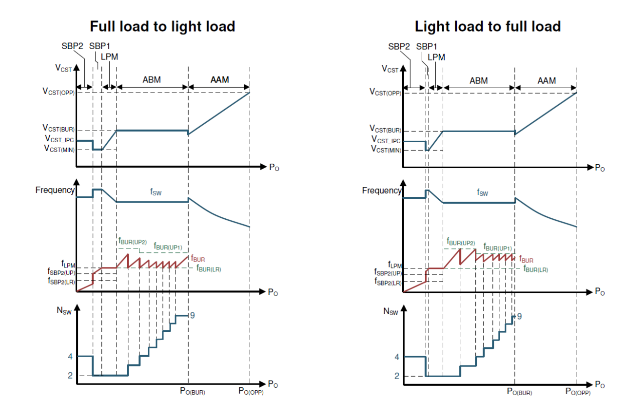
UCC28782 contains six modes of operation summarized in Table 2-1. Starting from heavier load, the AAM mode forces PWML and PWMH into complementary switching with ZVS tuning enabled. ABM mode generates a group of PWML and PWMH pulses as a burst packet, and adjusts the burst off-time to regulate the output voltage. At the same time, the burst frequency variation is confined above 20kHz by adjusting the number of PWML and PWMH pulses per packet to mitigate audible noise and reduce burst output ripple. In LPM, SBP1, and SBP2 modes, PWMH and the ZVS tuning loop are disabled, so the converter operates in valley-switching. The survival mode is to maintain VVDD higher than VVDD(OFF) in a long burst off time, and also performs the clamping capacitor balancing function to reduce the voltage stress of the secondary-side rectifier .
Table 2-1 and Figure 2-1 also show the frequency and power level at each mode, so it helps to understand the mode operation.
| MODE | OPERATION | PWMH | ZVS | |
|---|---|---|---|---|
| AAM | Adaptive Amplitude Modulation | ACF operation with PWML and PWMH in complementary switching | Enabled | Yes |
| ABM | Adaptive Burst Mode | Variable FBUR > FBUR(LR), ACF operation in complementary switching | Enabled | Yes |
| LPM | Low Power Mode | Fix FBUR ≈ FLPM, valley-switching | Disabled | No |
| SBP1 | First Standby Power Mode | Variable FBUR between FSBP2(LR) and FSBP2(UP), valley- switching | Disabled | No |
| SBP2 | Second Standby Power Mode | Variable FBUR< FSBP2(UP) as VBUR < 0.9 V; Variable FBUR< FSBP2(LR) as VBUR > 0.9 V; Both are in valley-switching | Disabled | No |
| INT_STOP | Survival Mode |
When VVDD < VVDD(OFF) + VVDD(PCT), a series of PWML pulses followed by a long PWMH pulse is generated |
Enabled in the lastswitching cycle of a survival-mode burst packet | No |
 Figure 2-1 Control Law Over Entire Load
Range Based on the VVS Condition as VIPC < 0.9
V
 Figure 2-2 Control Law Under Different
Load Sweep Direction as VIPC > 0.9 V and VVS >
VVSLV(UP)
Figure 2-2 Control Law Under Different
Load Sweep Direction as VIPC > 0.9 V and VVS >
VVSLV(UP)3 Design SOP and Checklist
TI has several publications and reference design to assist customers with designing the UCC28782. The following are some of the publications to assist with customer design.
Selecting the correct reference design as a starting point
Using calculator to design parameter
After choosing the correct reference design, the user can customize the parameter with their spec by calculator, UCC28782 calculator includes the IC parameter design and transformer design and secondary side resonance tuning and feedback loop design with TL431, so it is very helpful for customer to design the ACF board.
UCC28782 design calculator tool
Refer the layout guidelines with the data sheet section 11
Review the schematic and layout with checklist
The the schematic and layout design is completed, refer to the checklist shown in Table 3-1 and Table 3-2, so the user can double check that they did not miss any significant item.
UCC28782 system bring up guideline and debug FAQ
After the schematic and layout is finished, the user needs to evaluate the board, and might also face several issue. The user can refer to the application note for these item to speed up the debugging.
UCC28782 system timing up guideline and debug FAQ:
EMI filter design
After the system performance meets the spec without issue, the user needs to fine tune the EMI. TI has several application notes to assist with EMI tuning that include the following:
- Transformer structures that achieve low EMI with low and high side rectifiers
- Flyback Transformer Design for Efficiency and EMI
- Designing Low EMI Power Converters for Industrial and Automotive Systems
- Input EMI Filter Design for Offline Phase-Dimmable LED Power Supplies
| Checklist item | Purpose |
|---|---|
| The high-side driver with short power-on delay less than 10 μs | Make sure the high side GaN switching can follow PWMH signal immediately |
| Boostrap diode trr around 35ns | boostrap capacitor voltage charged quickly |
| Add 24 V or 27 V TVS at BIN pin | BIN and BSW pin voltage rating is 30V, so add TVS to prevent it damaged |
| Choice the boost inductor with higher than 0.4-A saturation current capability and DCR less than 1 Ω resistance | Prevent it trigger the survival mode easily |
| RVS1 using 0805 package | The voltage at RVS1 would up to 100V for 20V PD application |
| Choice the capacitor with low DC bias influenced at BIN, VDD, and Co1 | The capacitor may use 35V rating, but its capacitance is derating during 20Vo |
| Choice the optocoupler with higher CTR and low temperature variation, TLP383 or FODM8801A is suggested | Prevent the lower low frequency gain to suppress the AC ripple. |
| add the Rdiff and Cdiff at feedback loop | For dynamic load performance tuning |
| Add the bi-direction TVS diode at depletion FET GS pin | Protect the depletion FET |
| Reserve the Rrun and Drun | For LPM to ABM transition tuning |
| Add serial damping inductor with 1206 package | Improve the stability at ABM |
| SR MOS with 150 V rating for ACF 20V PD application,reserve the TVS at SR DS site | SR spike is observed at output voltage transition and SCP and LPM to ABM |
| Reserve the RC filter at high side GaN PWM input pin | Prevent the GaN fault turn on by noise |
| Completed | Layout Checklist |
|---|---|
| Minimize the power stage high dv/dt, di/dt, and dB/dt loop to prevent noise coupling to noise sensitive signals, and get better EMI performance | |
| GaN thermal dissipate by the PCB, make sure add enough via at GaN copper | |
| Avoid any trace overlap with VS pin trace, and minimize the VS pin trace | |
| Minimize these high dv/dt trace Vaux, BSW, and SWS to prevent noise coupling to noise sensitive signals | |
|
Make sure these component close to IC to minimize noise coupling: RRDM, RRTZ, RFB, CFB, RVS2, RBUR1, RBUR2, CBUR, Cref, CS pin RC filter, BIN pin TVS, CP13, CBIN2, and CVDD |
|
| Minimize the FB and CS loop to minimize noise coupling | |
| Csws and Dsws ground connect to Cbulk ground | |
| For GaN setting, RVS2 ground connect to SET pin and SET pin connect to thermal pad directly, and minimize the ground connection at set pin. | |
| AGND: the decoupling capacitors for REF, CS, BUR, and P13 connect to AGND, and use kelvin connection to Rsense return path. | |
| BGND: boost ground, CBIN, CVDD, and Auxwinding ground path connect to BGND, and connect to AGND at thermal pad or CVDD ground. | |
| PGND : gate driver return for PWML signal, if using the GaN with integrated gate driver, PGND connect to thermal pad directly, if not, connect to source pin of low side FET. | |
| Provide the shielding with ground planes on these pin : BUR pin and FB loop | |
| Avoide the shielding with ground planes on these pin : RDM, RTZ, and VS pin | |
| Make sure the RC filter for high side GaN PWM input pin close to GaN |