-
Reducing System Bill of Materials and MCU Pin Requirements With SPI eFuse Switches
Reducing System Bill of Materials and MCU Pin Requirements With SPI eFuse Switches
Power distribution electronic control units (ECUs), such as power distribution boxes and zone control modules (ZCM), require configurable and intelligent eFuse switches to remove dependency on the local microcontroller (MCU) to safely protect the wire harness. Additionally, ZCM MCU general purpose input and output (GPIO or I/O) and analog to digital converter (ADC) pins are limited due to the integration of additional vehicle functions that require the MCU to control or monitor numerous peripheral devices (load driver control, input management, diagnostics, and so on). Therefore, the TI HCS family of smart eFuse switches implement a serial peripheral interface (SPI) to provide flexible control and configuration of eFuse features such as fuse time-current profile, low-power mode, and capacitive charging modes discussed in detail within the Fully Software Configurable High Side Switch for Power Distribution Applications in Zone Controllers application brief. The integration of an ADC in combination with the SPI allows hardware design engineers to trim down the system bill of materials (BOM) directly decreasing cost and size of the overall eFuse design. Additionally, standard SPI and SPI daisy-chain configurations reduce the number of MCU pins and discrete I/O expander designs needed to control and monitor the eFuse outputs.
BOM Savings and MCU IO Reduction
The benefits of SPI are fully shown when compared to GPIO controlled eFuses and high side switches as shown in Figure 1.
 Figure 1 GPIO Versus SPI eFuse Switch
GPIO controlled devices require a minimum of four pins to control the device output and diagnostics. Multi-channel devices require an additional pin per output channel as well as pins for selecting which channel the analog output represents (for current measurements). Furthermore, GPIO controlled devices require filtering and clamping of the analog current sense output to reduce noise in the analog signal and protect the MCU ADC pin from over-voltage conditions (potentially seen during overcurrent events). For additional diagnostics, hardware engineers often add a BJT or MOSFET and resistors to the output to distinguish between short to battery or open load failure conditions. If the system needs to measure the output voltage, an additional voltage divider and ADC pin from the MCU are required. In contrast, the TPSxHCS family of efuses integrates an ADC in combination with SPI control to reduce the MCU pins needed for configuration, control, and diagnostics feedback. Therefore, the majority of passive components are no longer needed including the ADC filtering, fuse setting resistors, pull-up BJT/MOSFET, and voltage dividers. Additionally, no MCU ADC pins are required to measure the output current, output voltage, supply voltage, or FET temperature as these can be read through SPI. For an ECU that implements many peripheral devices, such as zone control modules, the MCU I/O and ADC pin are quickly consumed by GPIO controlled eFuse, high side switches, and other peripheral devices. Therefore, additional I/O expansion designs such as muxes (for analog signals), I2C or SPI I/O expanders, and/or shift registers are added. Figure 2 shows five single-channel eFuses driven by single-channel GPIO controlled eFuses with additional I/O expander and mux compared with the dual-channel TPS2HCSx-Q1 SPI eFuses.
 Figure 2 GPIO Versus SPI eFuse System Comparison
Each I/O expander adds components to the system BOM increasing cost. SPI eFuses allows multiple devices to share a single SPI port with each eFuse requiring an individual chip select pin (3xpins + 1xCS per eFuse). In addition to standard SPI implementation, the HCS family of eFuses include SPI daisy-chain configurations that allow for a single chip select pin to be shared across all eFuse devices in the chain. This enables control and diagnostic feedback from all eFuses with only 5 MCU pins. Table 1 summarizes the various approaches.
| eFuse Design | Number of Output Channels | MCU GPIO Pins | MCU ADC Pins | Number of ICs | Approximate eFuse Passive Components |
|---|---|---|---|---|---|
| GPIO eFuse | 5 | 16 | 5-10 | 5 | 1xFET/BJT, 60xResistors, 10xCapacitors, 10x Diodes |
| GPIO eFuse + IO Expanders | 5 | 8-10 | 1 | 7 | 1xFET/BJT, 47xResistors, 1xCapacitors, 6x Diodes |
| SPI eFuse Standard | 6 | 7 | 0 | 3 | 18xResistors, 3xCapcitors |
| SPI eFuse Daisy-Chain | 6 | 5 | 0 | 3 | 18xResistors, 3xCapcitors |
The 2 additional I/O expander integrated circuits (ICs) reduce the MCU pins required by 12 to 15 and further help reduce the passive components by 26. In contrast, the standard SPI configuration reduces the MCU pins by 14 to 19, requires 45 fewer passive components and does not require additional I/O expansion ICs. The SPI daisy-chain further reduces the MCU pins by 16 to 21. With SPI daisy-chain only 5 pins are ever required further reducing the GPIO and ADC pin savings if more eFuse devices are added to the chain.
SPI Daisy Chain Test Results
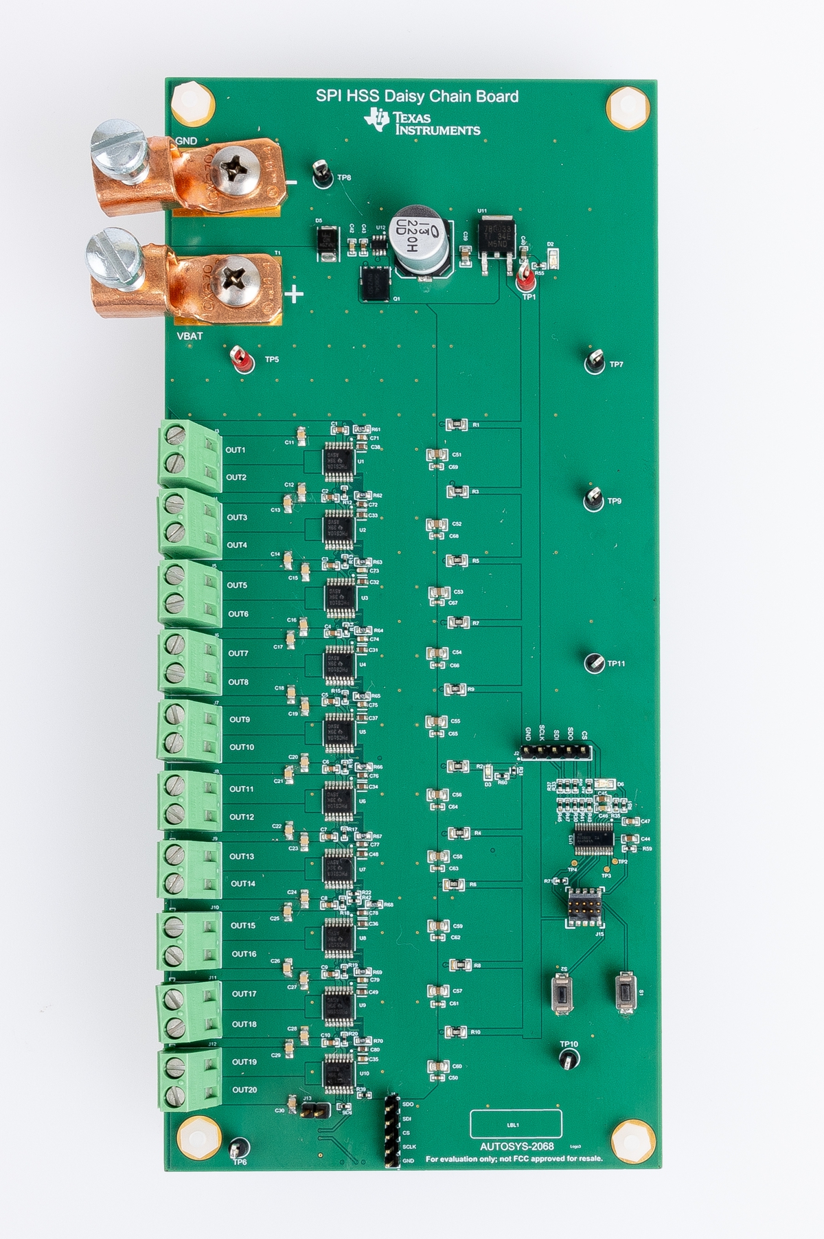
Figure 3 shows the PCB created for testing TPS2HCS10-Q1 daisy-chain SPI capabilities. A total of 10 dual-channel eFuse switches are implemented on the PCB with options to daisy chain 4, 6, 8, or 10 devices. The eFuse devices can also be split into two different daisy chains of four and six devices per chain.
 Figure 3 Board Photo
Table 2 summarizes the latency timing data collected for daisy-chain configurations of 4, 6, and 10 devices. Each configuration was tested with SPI clock frequencies of 2MHz, 4MHz, and 8MHz and with the MCU (MSPM0G) core clock operating at 80MHz.
| Number of Devices | SPI Frequency (MHz) | Expected Read Latency (us) | Measured Read Latency (us) | Expected Write Latency (us) | Measured Write Latency (us) |
|---|---|---|---|---|---|
| 4 | 2 | 96 | 105.9 | 48 | 49.70 |
| 4 | 48 | 58.61 | 24 | 25.79 | |
| 8 | 24 | 34.81 | 12 | 13.892 | |
| 6 | 2 | 144 | 155.70 | 72 | 73.55 |
| 4 | 72 | 85.17 | 36 | 37.89 | |
| 8 | 36 | 49.49 | 18 | 20.06 | |
| 10 | 2 | 240 | 244.12 | 120 | 120.98 |
| 4 | 120 | 124.78 | 60 | 61.55 | |
| 8 | 60 | 65.32 | 30 | 31.71 |
Figure 4 shows an example of sending read commands to 10 devices in a daisy chain. First, a read command is sent to 10 TPS2HCS10-Q1 devices. Another read command must be sent because the data on SDO corresponds to the data for the previous SPI transaction, therefore, the latency is measured as the length of 2 SPI transactions. The SPI clock is also set to 8MHz for this test.
 Figure 4 10 Device Daisy Chain Timing
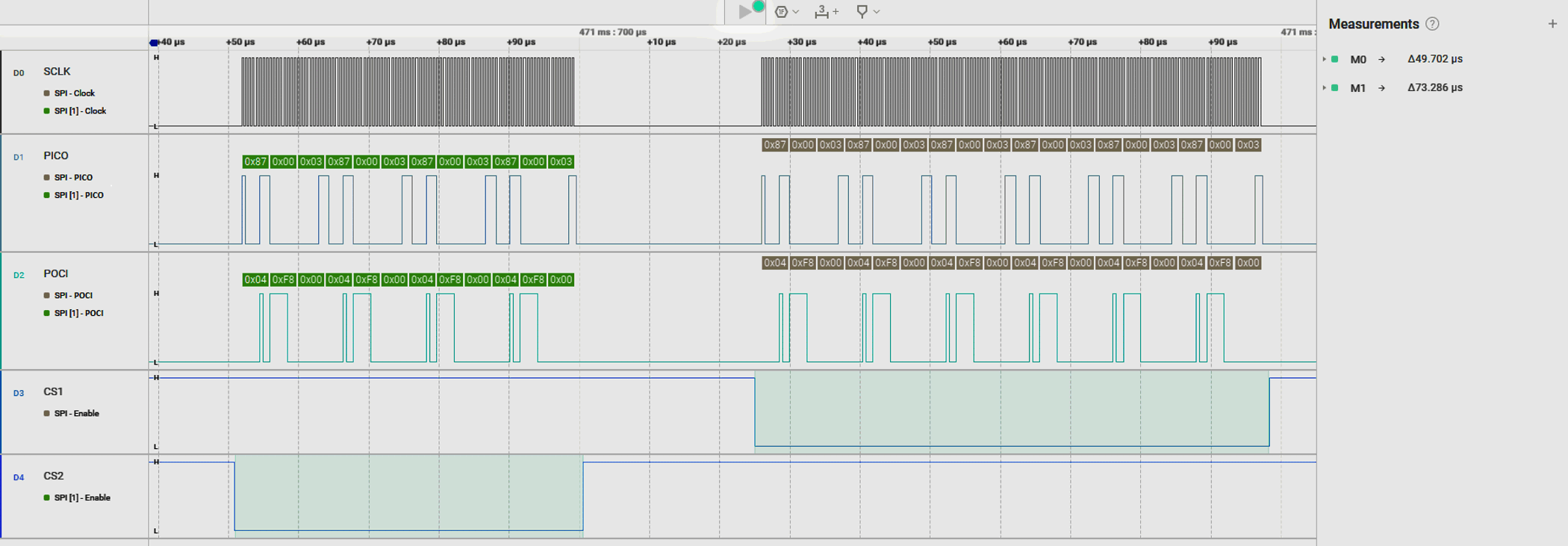
Additional tests were done to show a configuration involving multiple daisy chains. As shown in Figure 5, write commands are sent to enable all outputs on one daisy chain of four devices and another daisy chain of six devices. The SPI clock for this test was set to 2MHz.
 Figure 5 Dual Daisy Chain Timing
An additional factor that contributes to the latency measurements is the MCU software overhead needed in between SPI commands. For the previous tests shown, 80MHz was used for the operating core clock frequency to decrease the overhead time. Direct memory access (DMA) controllers were also used to reduce this delay by allowing the transfer of data between the SPI TX and RX FIFO independent of the CPU. Figure 6 shows a write transaction with a SPI clock of 8MHz performed with a core clock of 32MHz. Comparing this result to Figure 4, the latency is reduced by about 16us. For a read command, the latency is reduced by about 32us.
 Figure 6 10 Device Daisy Chain Timing (Core Clock = 32MHz)
Trademarks
All trademarks are the property of their respective owners.
IMPORTANT NOTICE AND DISCLAIMER
TI PROVIDES TECHNICAL AND RELIABILITY DATA (INCLUDING DATASHEETS), DESIGN RESOURCES (INCLUDING REFERENCE DESIGNS), APPLICATION OR OTHER DESIGN ADVICE, WEB TOOLS, SAFETY INFORMATION, AND OTHER RESOURCES “AS IS” AND WITH ALL FAULTS, AND DISCLAIMS ALL WARRANTIES, EXPRESS AND IMPLIED, INCLUDING WITHOUT LIMITATION ANY IMPLIED WARRANTIES OF MERCHANTABILITY, FITNESS FOR A PARTICULAR PURPOSE OR NON-INFRINGEMENT OF THIRD PARTY INTELLECTUAL PROPERTY RIGHTS.
These resources are intended for skilled developers designing with TI products. You are solely responsible for (1) selecting the appropriate TI products for your application, (2) designing, validating and testing your application, and (3) ensuring your application meets applicable standards, and any other safety, security, or other requirements. These resources are subject to change without notice. TI grants you permission to use these resources only for development of an application that uses the TI products described in the resource. Other reproduction and display of these resources is prohibited. No license is granted to any other TI intellectual property right or to any third party intellectual property right. TI disclaims responsibility for, and you will fully indemnify TI and its representatives against, any claims, damages, costs, losses, and liabilities arising out of your use of these resources.
TI’s products are provided subject to TI’s Terms of Sale (www.ti.com/legal/termsofsale.html) or other applicable terms available either on ti.com or provided in conjunction with such TI products. TI’s provision of these resources does not expand or otherwise alter TI’s applicable warranties or warranty disclaimers for TI products.
Mailing Address: Texas Instruments, Post Office Box 655303, Dallas, Texas 75265
Copyright © 2024, Texas Instruments Incorporated