-
3 Ways to Reduce Power-supply Noise with Power Modules SSZT209 December 2020 TPSM41615 , TPSM41625 , TPSM5D1806 , TPSM846C23
-
3 Ways to Reduce Power-supply Noise with Power Modules
3 Ways to Reduce Power-supply Noise with Power Modules
Sheetal Liddar
Noise is an unwelcomed electrical phenomenon that commonly originates in the power supply. If not reduced, noise can adversely impact the performance of applications in sensitive medical, test and measurement, and aerospace and defense systems.
Today’s high-precision analog signal-chain systems require DC/DC switching regulators to generate regulated power-supply rails for powering analog-to-digital converters (ADCs), digital-to-analog converters (DACs), field-programmable grid arrays (FPGAs) and their subsystems in low-noise applications. While DC/DC switching regulators are efficient, their switching action results in large discontinuous currents, which generate high input and output voltage ripples, frequency spikes and wideband noise. If not controlled to the ADC or DAC’s least-significant-bit millivolt range, these discontinuous currents can affect system accuracy.
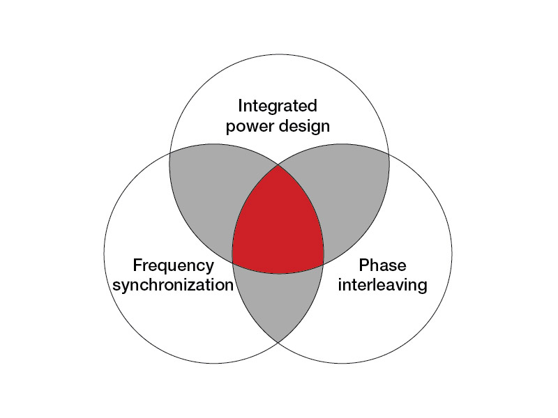
This article focuses on three ways that buck power modules can help with noise reduction: removing parasitics through an integrated module design, mitigating undesired beat frequency and inaccuracies with frequency synchronization, and lowering the input ripple current and output voltage ripple through phase interleaving. DC/DC buck power modules with all three features, as shown in Figure 1, can help significantly lower the noise of your power supply for low-noise applications.
 Figure 1 Venn diagram of desirable
DC/DC buck module features for low noise
Figure 1 Venn diagram of desirable
DC/DC buck module features for low noiseRemoving parasitics through an integrated module design
Most noise problems with switching power supplies are associated with the parasitic components of the design. When using a DC/DC switching regulator, you have to add external components such as input capacitors, inductors and output capacitors to form a closed loop. Placing these external components far from the switching regulator on the board results in board parasitics at the VIN and SW nodes. These parasitics create a high transient current (di/dt) loop, as shown in Figure 2. In a loop in which currents suddenly turn on and off during switching, high-frequency ringing (switching noise) occurs.
Buck power modules with an integrated controller, FETs, an inductor and bypass capacitors are designed with optimized layouts to help minimize these board parasitics. A buck power module’s advanced package construction enables the integration of bypass capacitors closer to the VIN and VOUT pins, and the placement of inductors closer to the SW node (in some cases, on top of the converter in a 3D construction style). Designing the overall layout and routing of internal components with the goal to reduce the high di/dt loop area and transient voltage (dv/dt) node area helps minimize the input and output ripple voltages.
 Figure 2 The di/dt loop for a discrete converter (a) vs. a buck power module (b)
Mitigating undesired beat frequency and inaccuracies with frequency synchronization
Input and output noise becomes a challenge when designing multiple switching converters into the same application. The challenge multiplies when a converter’s switching frequencies change with the input voltage and output load. Even with fixed-frequency operation of each converter, the frequency tolerance of the different converters can result in an undesirable beat frequency (a difference of switching frequency).
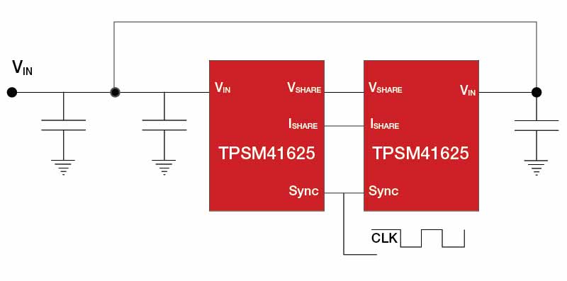
To overcome switching frequency inaccuracy and beat frequencies, some buck power modules provide an external SYNC pin that enables the synchronization of one or more regulators to a common system clock. Synchronizing all modules to an external clock like shown in Figure 3 can lower the input current and voltage ripple at a particular system clock frequency, which can further reduce the need for noise filtering and result in less total capacitance for a module. Synchronizing all buck power modules to a central system clock can also prevent them from interfering with sensitive analog or digital sections of the overall system.
 Figure 3 Two buck power modules synchronized to a system clock
Lowering the input ripple current and output voltage ripple through phase interleaving
While synchronizing all buck power modules can help lower noise and avoid beat frequencies, it can sometimes place stress on the input capacitors. In a synchronized system, all buck regulators draw pulse currents at the onset of the system clock, which can result in a large root-mean-square current stressing the input capacitors thermally. It can also contribute to noise peaks in the system.
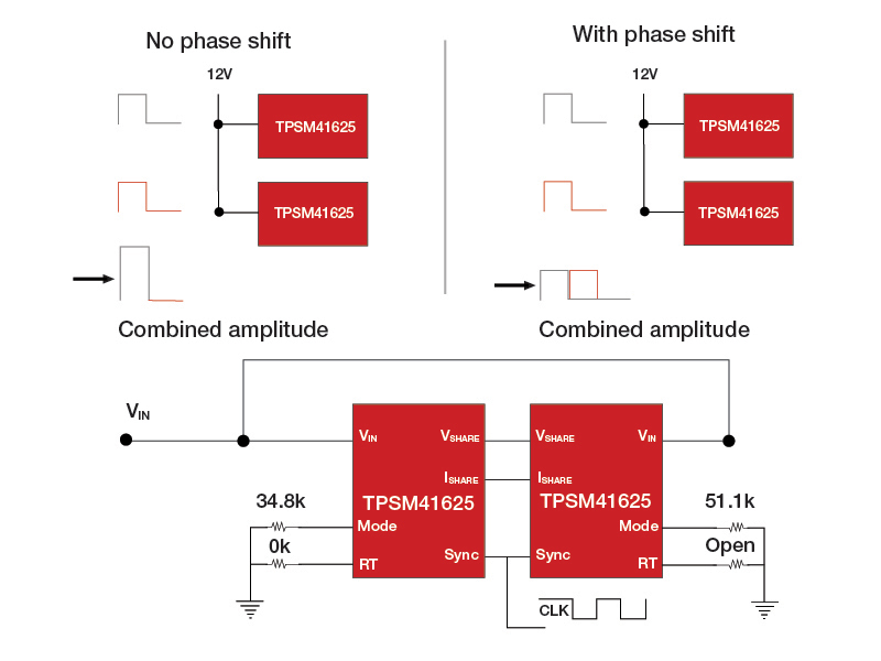
To address this issue, consider phase interleaving, where the clock edges are delayed to arrive at different buck power modules at different times within the system clock cycle. By doing this, the demand for pulse current at the input shifts in time, as depicted in Figure 4, for no-phase-shift and with-phase-shift configurations. This implementation can help lower the input current and output voltage ripple at a defined frequency, thereby reducing efforts for noise filtering.
 Figure 4 A 180-Degree Phase-shift Synchronized TPSM41625 Modules
Conclusion
Low-noise switching power supplies come in many flavors. If you like working with modules and know what to look for, you can effectively reduce your power-supply noise. Consider selecting buck power modules that offer frequency synchronization and phase interleaving when designing your next low-noise multirail power supply for ADCs, DACs and FPGAs.
Additional resources
- Check out these application notes to learn more:
- Learn more about multiphase buck converters in the Analog Design Journal article, “Benefits of a multiphase buck converter.”
IMPORTANT NOTICE AND DISCLAIMER
TI PROVIDES TECHNICAL AND RELIABILITY DATA (INCLUDING DATASHEETS), DESIGN RESOURCES (INCLUDING REFERENCE DESIGNS), APPLICATION OR OTHER DESIGN ADVICE, WEB TOOLS, SAFETY INFORMATION, AND OTHER RESOURCES “AS IS” AND WITH ALL FAULTS, AND DISCLAIMS ALL WARRANTIES, EXPRESS AND IMPLIED, INCLUDING WITHOUT LIMITATION ANY IMPLIED WARRANTIES OF MERCHANTABILITY, FITNESS FOR A PARTICULAR PURPOSE OR NON-INFRINGEMENT OF THIRD PARTY INTELLECTUAL PROPERTY RIGHTS.
These resources are intended for skilled developers designing with TI products. You are solely responsible for (1) selecting the appropriate TI products for your application, (2) designing, validating and testing your application, and (3) ensuring your application meets applicable standards, and any other safety, security, or other requirements. These resources are subject to change without notice. TI grants you permission to use these resources only for development of an application that uses the TI products described in the resource. Other reproduction and display of these resources is prohibited. No license is granted to any other TI intellectual property right or to any third party intellectual property right. TI disclaims responsibility for, and you will fully indemnify TI and its representatives against, any claims, damages, costs, losses, and liabilities arising out of your use of these resources.
TI’s products are provided subject to TI’s Terms of Sale (www.ti.com/legal/termsofsale.html) or other applicable terms available either on ti.com or provided in conjunction with such TI products. TI’s provision of these resources does not expand or otherwise alter TI’s applicable warranties or warranty disclaimers for TI products.
Mailing Address: Texas Instruments, Post Office Box 655303, Dallas, Texas 75265
Copyright © 2023, Texas Instruments Incorporated